

Get the semiconductor daily news directly to you by subscribing to our email list. For ASIC designer and managers, staying updated with the latest news, technologies, and trends is crucial. Here are the lastest news from the semiconductor industry.

As technologies advance, the semiconductor industry and its traditional business model face a myriad of ongoing complexities demanding an ever accelerating state of operational agility. The electronics and healthcare markets are experiencing unprecedented change through mass market consumerization and global adoption. For most chip companies, gone are the days of
Read More
Over the last 5 years lead generation has fundamentally changed. Companies used to participate in expensive events and focus mostly on branding activities. But today potential customers have direct access to all the products information they need, things are different.
In other industries, marketing & sales teams understand that their
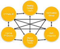
hat comes to mind when you hear the term IP Distribution? How do people like ARM and MIPS get their cores into people’s hands? Pricing, contracts and legal issues? Maybe third-party Web sites like Chip Estimate and Design & Reuse? Yes, they are all factors in how independently developed IP
Read More
The CMOS Image Sensor (CIS) industry reaches US$10B for the first time. Indeed, driven by mobile and automotive applications, the CIS industry is expected to grow at a CAGR of 10.6% from 2014 – 2020. Yole Développement (Yole) announces a US$16.2B market by 2020 (in value):
“Smartphone applications still take the lion’s
As everybody is trying to figure out what the Internet of Things (IoT) will look like and how connected things will work, I’d like to address a question that many people have: why design your own Integrated Circuit (IC) rather than just use an off-the-shelf processor, write software and be done?
In a

Recently we worked with a customer that had an urgent need to get a custom analog ASIC (application specific integrated circuit) developed in a very short time. The customer needed a completely working system in the first quarter of 2015. Working backwards from their system schedule they realized that they
Read More
Clock to an SoC is like blood to a human body. Just the way blood flows to each and every part of the body and regulates metabolism, clock reaches each and every sequential device and controls the digital events inside the SoC. There are many terms which modern designers use
Read More
I think this is an appropriate first post, because this is a question that we’ve heard many times when talking with hardware engineers trying to sell our product. The fact that there are (now) about a dozen companies trying to replace RTL with alternatives (I’ll talk about HLS in other
Read More
The ultimate ASIC calculator is available live on AnySilicon’s website. Together with our Die Per Wafer calculator this ASIC price calculator provides a very accurate final price for ASIC designs. Please note, we did not include shipping cost therefore you may want to add this to the total prices.
Read More
Die Per Wafer (DPW) online calculator is free and available live on AnySilicon website. The die per wafer calculator is simple to use and very accurate, however the results are estimates.
Now when you have the number of dies per wafer, you may want to consider:
See