

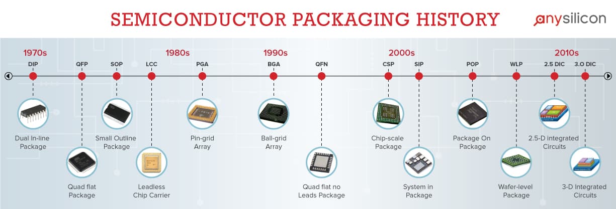
Since the invention of the first semiconductor package in 1965, the semiconductor packaging technology has grown dramatically and several thousands of different semiconductor package types have been made. The chart below presents the semiconductor packaging history. Particularly it shows the two major trends in semiconductor packaging: addressing high pin count and accommodating small footprint requirements.
Read more about semiconductor packaging: The Ultimate Guide to Semiconductor Packaging
Semiconductor package enables electrical connection between the silicon die and the PCB. The package helps fanning out the dense die pads into larger area so PCB layout and assembly can be made easily.
In power hungry applications the semiconductor package responsibility is to dissipate the heat produced by the silicon die to a large surface, such as heat sink. This allows the die to continue operate normally in high temperature environments.
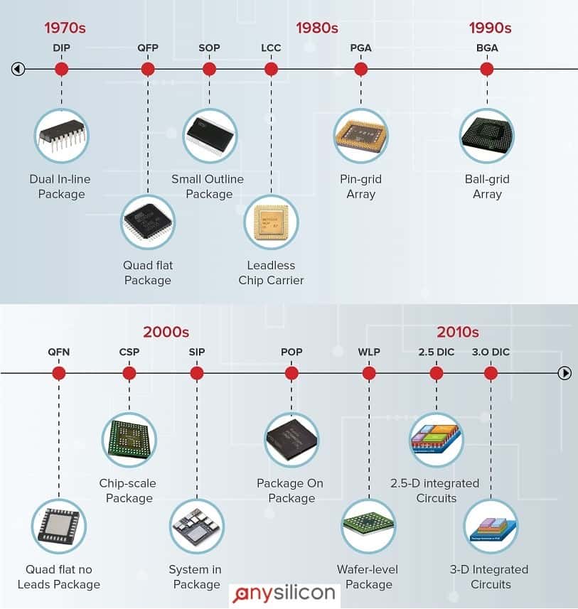
Three engineers from Fairchild: Don Forbes, Rex Rice, and Bryant Rogers invented a 14-lead ceramic Dual-in-Line Package (DIP) with two rows of pins. This was the first real semiconductor package. DIP packages came into volume production in early 70’s.
In the 80’s, chips became larger and integrated more functionality. A chip with 1 million gates was introduced and the semiconductor packaging technology had to address the increasing number of IOs. This was the reason for introducing PGA (Pin Grid Array) and BGA (Ball Grid Array) packages.
Addressing the high IOs was driven mostly by high-end SoCs used for computing, networking, and storage application when large data or address buses are needed for transferring data in and out the chip. The struggle in these type of applications is balancing between size, power dissipation and cost.
In the beginning, every BGA/PGA package was based on a ceramic substrate but today laminate is a primary source for both low cost and high end applications. Laminate is a low cost solution for BGA substrates that can support both low and high performance applications.
In the 90’s the CSP (Chip Scale Package) was introduced to address both high pin count and small size requirements. The CSP package is essentially a small size BGA with smaller ball pitch.
In the 90’s the second trend in semiconductor packaging has started and it was all about miniaturization. This trend was obviously driven by mobile devices such as laptop and mobile phones which demanded “near die size” type of packages in order to eliminate package cost and area.
Due to these requirements several packaging technologies were introduced. QFN package was introduce as a type of CSP (Chip Scale Package) and since, QFN package has become the most successful package type because of its simplicity, performance and price.
WLCSP (bumping) package type was also developed and it’s currently the smallest size package because the package size equal the die size.
Download this chart by using this link.
Need a price quote for your IC/SoC packaging? Get 3 quotes quickly using this form.
Get an indicative packaging cost range, then a detailed breakdown by email.
