

Semiconductor packaging is a crucial aspect of electronics manufacturing that involves enclosing semiconductor chips in protective and functional packages to ensure their reliability, performance and integration into electronic devices. These packages serve as a bridge between the tiny, sensitive semiconductor chips and the broader electronic systems, providing electrical connections, thermal management, and environmental protection. Semiconductor packaging technologies have evolved significantly to meet the demands of smaller, faster, and more efficient electronic devices, ranging from traditional leaded packages to advanced flip-chip, system-in-package (SiP), and 3D packaging. These packaging innovations play a vital role in powering a wide range of modern applications, from smartphones and IoT devices to data centers and automotive electronics.
In the formative years of semiconductor industry, semiconductor devices were packaged using metal cans and ceramic packages. These packages served the purpose of providing basic protection for the delicate semiconductor chips and allowed for electrical connections to the external circuitry. However, they were relatively large, bulky, and had limited functionality. As semiconductor technology advanced rapidly, there was a growing demand for smaller, more efficient packaging solutions to match the shrinking size of semiconductor chips. This led to the development of innovative packaging techniques like dual-in-line packages (DIPs) and surface-mount packages. Dual-in-line packages could not support high pin-counts and there was a need for high-density interconnect (HDI) solution that can accommodate a great number of IOs. This gave birth to flip chip packages, also known as Controlled Collapse Chip Connection (C4). In order to attain high levels of integration, designers came up with MCM (Multi-Chip Module) around 1970s.
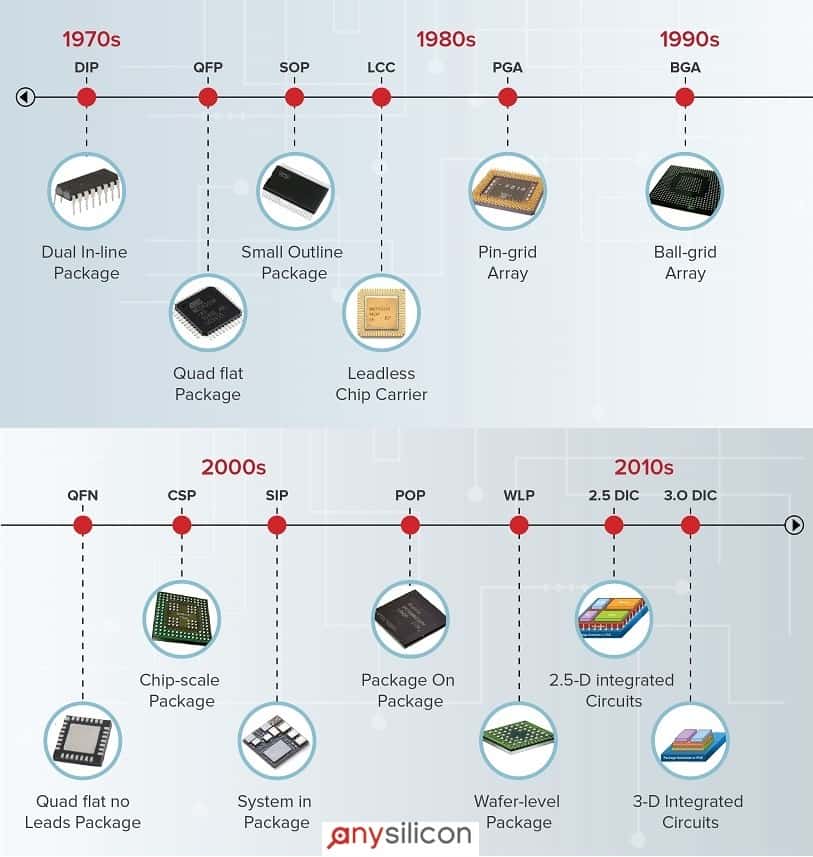
Figure 1: History of semiconductor packaging
Semiconductor packaging materials play a crucial role in protecting and interconnecting devices while ensuring their reliability and performance.
Substrates: Substrates can be organic or ceramic. Organic substrates have great electrical insulation properties and are cost effective packaging solution. Ceramic substrates are typically used in high-frequency applications that demand good thermal conductivity.
Encapsulation Materials: Encapsulating materials protect the chips from environmental factors, moisture, and mechanical stress. Epoxy Molding Compound (EMC) offers good adhesion and has good electrical insulation properties. However, Liquid Crystal Polymer (LCP) is more suitable for high frequency applications due to its low dielectric constant and low loss tangent.
Interconnect Materials: Gold wire bonding is typically used to make electrical connections between the semiconductor chip and the package. Lead-free solder (Tin-silver-copper alloy) materials are used for attaching semiconductor chips to substrates.
Underfill Materials: Underfill materials are applied to fill the gap between the semiconductor chip and the substrate to enhance mechanical stability and reliability. Underfill materials also improve the thermal conductivity by allowing for better heat dissipation and reducing the risk of overheating. Typical materials of choice are epoxy resins (for better adhesion), polyimides (better thermal stability) or silicones (better mechanical stability).
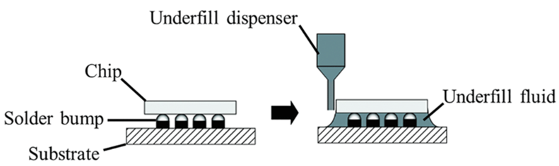
Figure 2: Flip-chip underfill encapsulation process
The Quad Flat Package is a classic semiconductor package characterized by its flat, square or rectangular shape with leads extending from all four sides. QFPs come in various sizes, with pins arranged in a grid pattern. They are commonly used for integrated circuits (ICs) that require moderate pin counts. QFPs offer ease of handling during assembly and rework.
Ball Grid Array packages feature an array of solder balls on the underside of the package instead of leads. These solder balls make contact with corresponding pads on the PCB, enhancing thermal performance and reducing the risk of electrical interference. BGAs are widely used in modern electronics due to their compact size, excellent heat dissipation capabilities, and resistance to mechanical stress.

Chip-scale packages are designed to be nearly the same size as the semiconductor chip they enclose, minimizing wasted space. CSPs are ideal for applications where size and weight constraints are critical, such as in mobile devices and wearables. They often use very fine-pitch solder balls or copper pillars for connections.
Wafer-level packaging is a technique where multiple semiconductor devices are packaged at the wafer level before they are diced into individual chips. This approach can reduce manufacturing costs and improve device performance. WLP allows for the creation of ultra-compact and high-density packages, making it suitable for applications like MEMS devices and sensors. Read more about wafer level packaging here.
3D IC packaging involves stacking multiple semiconductor die on top of each other within a single package, interconnected using through-silicon vias (TSVs). This packaging technology enables higher levels of integration, reduced signal delays, and enhanced performance. Stacked packages are used in advanced applications like high-performance computing, graphics cards, and memory modules to boost processing power and memory capacity while conserving space.
Semiconductor package design is a complex and evolving field that faces various challenges in today’s rapidly advancing technology landscape. Here are the top challenges:
Miniaturization and Integration: In accordance with Moore’s Law, the electronic devices are becoming smaller and more powerful. It becomes challenging for the package design to keep up with the miniaturization and integration while maintaining the performance and the reliability of the package.
With less space for components and interconnects on the package, dealing with issues like signal integrity, power delivery and thermal management presents unique challenges that requires innovative solutions.
Thermal Management: The incessant demand for high performance while reducing the overall area translates into high power densities on the IC. Overheating can reduce the lifespan of ICs and affect performance. Packages are designed to better dissipate the heat and advanced thermal solutions such as heat sinks, heat spreaders and advanced thermal interface materials are critical for dissipating heat efficiently. Additionally, 3D packaging and integrated cooling solutions are emerging to address these challenges by providing pathways for better heat dissipation.
Advanced Materials and Compatibility: Semiconductor industry seeks to design packages using materials with improved electrical, mechanical, and thermal properties. The package needs to interface with other materials like silicon, organic substrates, and solder, which can have different thermal expansion coefficients (CTE). These differences can result in thermal stresses during temperature cycling, potentially leading to package failure. Using low-CTE materials like Copper Tungsten (CuW), Aluminum Silicon Carbide (AlSiC), Kovar etc. can reduce the impact of thermal mismatches and improve the package reliability.
Signal Integrity and Electrical Performance: With increasing data rates and processing speeds, maintaining signal integrity and electrical performance in semiconductor packages becomes more demanding. High frequency signals are susceptible to interference, crosstalk and impedance mismatches. Designers need to consider factors like transmission line effects, electromagnetic interference (EMI), and power integrity to ensure that signals reach their destinations without distortion or loss.
Package Cost: Packaging can account for a significant portion of the overall cost of semiconductor devices. To make the parts competitive and also affordable for the consumers, design houses strive to reduce the packaging costs while maintaining performance. Click here to get a package cost.
Environmental Concerns: Electronic waste has a deleterious impact on environment and human health. There has been a push towards using environment friendly materials and recyclable materials for semiconductor package.
Heterogenous Integration: Integrating different technologies like memory, sensors, radio-frequency (RF) components into a single package is known as heterogenous integration. This offers many advantages including improved data transfer rates, reduced power consumption, enhanced device performance and occupies smaller space. Heterogenous integration presents unique challenges due to issues related to material compatibility between different technologies and managing thermal hotspots caused by diverse components operating at different power levels.
The challenges with semiconductor packaging open offers opportunities for innovation to thrive. Following are some of the advanced packaging techniques that are in use today:
System-in-Package (SiP): SiP is an advanced semiconductor packaging technology that integrates multiple heterogenous semiconductor components such as logic components (microcontroller or application processor chips, memories etc.), passive components (resistors, capacitors and inductors), memory components and interconnects (microbumps, wire bonds or TSVs) within a single package. SiP offers many advantages:
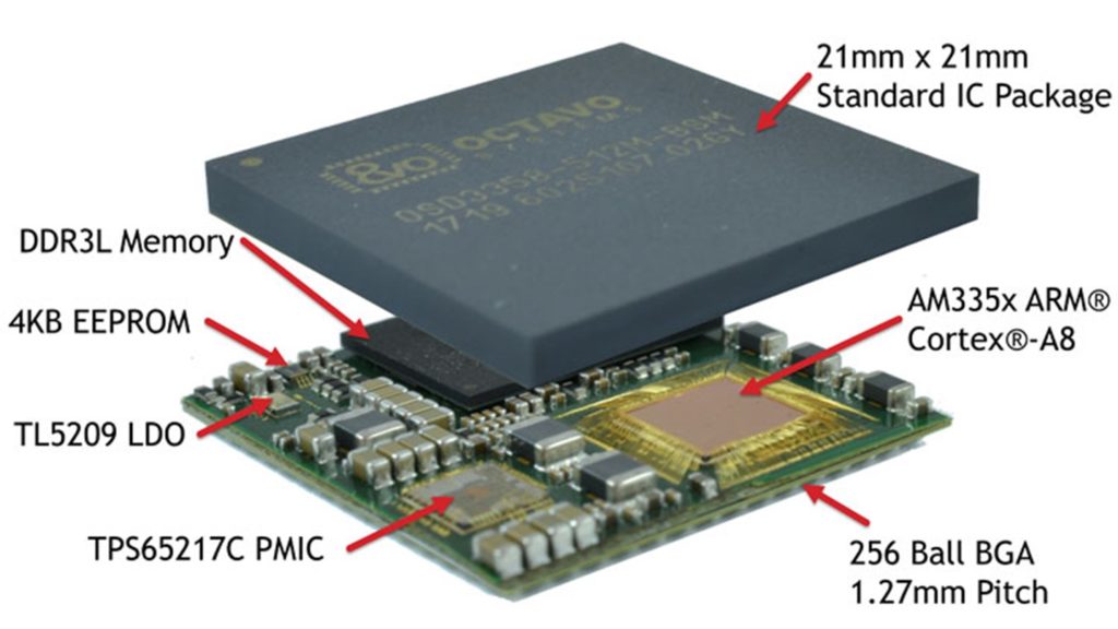
Figure 3: System in Package (SiP)
Fan-Out Wafer-Level Packaging (FOWLP): Traditional packaging methods involved packaging individual chips and mounting them on a printed circuit board. FOWLP involves redistributing and placing the chips face-up on a large wafer-sized substrate. This redistribution allows for the creation of compact, highly integrated packages that can include multiple chips, passive components, and interconnects within a single structure where the electrical connections are on the chip’s active side, connecting to the substrate.
It offers advantages such as miniaturization, improved thermal performance, cost-effectiveness, and enhanced electrical performance, making it a popular choice for a wide range of applications including smartphones, IoT devices, automotive electronics, and RF modules.
Through Silicon Vias (TSVs) and 3D IC packages: Through Silicon Vias (TSVs) are a critical technology used in 3D integrated circuits that enable vertical integration of multiple semiconductor dies or layers within a single package. TSVs are vertical interconnects that penetrate through the silicon substrate, providing electrical connections between different layers of chips of components.
TSVs are cylindrical or vertical holes that pass through the silicon substrate of each chip or layer in the 3D IC stack. They are lined with insulating material to prevent electrical shorts and are filled with a conductive material such as copper or tungsten to provide electrical pathways.
Vertical integration has helped revitalize transistor scaling by allowing multiple dies to be vertically stacked on top of each other. This helps reduce the interconnect lengths, increasing the integration density while also enhancing the power efficiency.
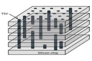
Figure 4: Through Silicon Vias (TSVs) for 3D Integrated Circuits
Embedded Multi-die Interconnect Bridge (EMIB): EMIB is an advanced semiconductor packaging technology developed by Intel. EMIB technology is designed to address the challenges of integrating heterogenous semiconductor dies within a single package. It uses an embedded bridge that spans across the substrate, thereby providing a high-speed, low latency pathway for data transfer between the integrated dies. It also uses fine-pitch interconnects such as micro-pillars to establish the electrical connections between the integrated dies. This enables efficient data transfer by reducing signal delays and improves electrical performance due to shorter interconnect lengths.
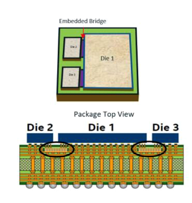
Figure 5: EMIB Technology by Intel
In conclusion, semiconductor packaging serves as the vital bridge between the intricate world of semiconductor chips and the diverse landscape of electronic devices that power our modern lives. From the early days of metal cans to the cutting-edge developments in 3D integration, semiconductor packaging has transformed our world, enabling the devices that connect us, entertain us and drive our industries.
References:
Get an indicative packaging cost range, then a detailed breakdown by email.


