

At the cornerstone of the semiconductor manufacturing process lies the Front End of Line (FEOL), which marks the beginning of this rigorous journey. The FEOL comprises fundamental steps like wafer cleaning, oxidation, and lithography, all essential in crafting the basic structures of semiconductor devices. Its influence spreads to device performance, efficiency, and ultimately, impacts the yield of functional units.
The journey doesn’t end with FEOL; it serves as a launchpad for subsequent processes, such as the Mid End of Line (MEOL) and Back End of Line (BEOL), that complete the semiconductor’s lifecycle. This article will delve into the complexities of FEOL, its key components, its pivotal role in electronics, and the challenges it faces, offering insights into the ever-evolving world of semiconductor technology.
Semiconductor manufacturing is a complex process that transforms silicon wafers into the functional chips found in electronic devices. This intricate procedure involves many steps, each crucial in ensuring the chips’ quality and effectiveness. A notable part of this process is the creation of a protective layer of silicon dioxide to shield the chips. Semiconductor manufacturing requires precision to form metal layers for connections and gate stacks to control electrical properties. Each wafer surface must be meticulously prepared in a cleanroom environment to prevent contamination and ensure reliability. The entire process involves chemical solutions and lithography to craft the detailed structures needed for modern chips.
The Role of Semiconductor Devices
Semiconductor devices play an essential role in modern electronics by controlling the flow of electricity. These devices are the brain of electronic gadgets, from smartphones to computers. They rely on semiconductor manufacturing to build individual chips that perform specific functions. The process includes creating basic structures using dielectric material to manage electrical pathways. Additional metal layers form a metal interconnect layer, ensuring signals travel efficiently across memory chips. These devices must be carefully designed and manufactured to meet the complex tasks of today’s technology while balancing aspect ratio structures for optimal performance.
Importance of Manufacturing Stages
The manufacturing stages of semiconductors are vital for producing reliable and efficient chips. Each stage is designed to refine the characteristics of the chips, from initial silicon wafer preparation to final chip packaging. First, the wafers receive a protective layer to combat unwanted silicon dioxide formation. Then, throughout the process, layers are meticulously added, including gate dielectric and Additional Metal Layers. The lithography process ensures accurate placement of these components. Ensuring these steps are performed correctly during the entire process affects the chip’s final effectiveness and stability. Therefore, every stage requires precision to create the complex structures central to modern electronics.
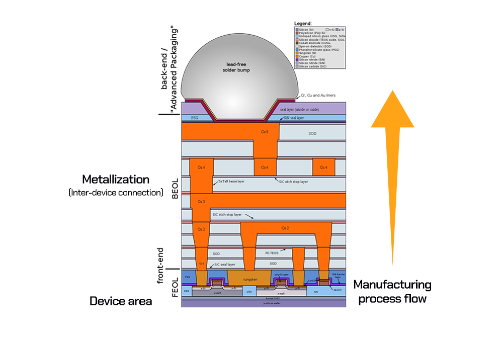
The Front End of Line, or FEOL, is a crucial stage in the semiconductor manufacturing process. It involves the creation of transistors on semiconductor silicon wafers. FEOL focuses on forming the electronic device structures that control a chip’s basic functions. This stage begins with the wafer surface, where layers of silicon dioxide are formed. These serve as a protective layer and are essential to the electrical properties of the chip. The FEOL process is complex and requires precision to ensure that each layer is created correctly. Understanding this process is critical for designing modern chips that perform efficiently and reliably. As the first stage in chip manufacturing, FEOL sets the foundation for the subsequent stages, including the Back End of Line (BEOL) and chip packaging.
Key Components of FEOL
The Front End of Line (FEOL) is a critical stage in the semiconductor manufacturing process. It involves preparing the silicon wafers for building electronic devices. Here are the key components:
The entire process must be precise to ensure the correct electrical properties for the individual chips. These steps lay the foundation for the metal interconnect layer in the later stages of chip manufacturing.
Key Processes in FEOL
The Front End of Line (FEOL) is the first phase in semiconductor manufacturing, focused on preparing silicon wafers. This stage sets the stage for future processes that develop the final chip. Each step in FEOL is integral to building a robust electronic device. From initial wafer cleaning to complex lithography, these processes ensure high-quality chips. The FEOL is essential for establishing the electrical properties needed for the device to function. By understanding these key processes, one can appreciate the intricacies involved in chip manufacturing. Let’s delve into the main components of FEOL.
Wafer Cleaning
Wafer cleaning is the starting point of the FEOL. It’s vital to remove impurities from the wafer surface. These impurities can be dust, unwanted silicon dioxide, or any residue left from previous processes. A clean wafer ensures that subsequent layers adhere properly and that the electrical properties are not compromised.
A cleanroom environment is crucial during this step. Here, workers use chemical solutions to clean the wafer thoroughly. These solutions dissolve particles and contaminants without damaging the wafer. This ensures that the silicon surface is smooth and ready for the next steps. Attention to detail during cleaning is crucial, as even the smallest contaminant can affect the entire process.
Oxidation
In the oxidation process, a thin layer of silicon dioxide forms on the surface of the wafer. This oxide layer plays a crucial role in protecting the wafer during various stages. It serves as the gate dielectric in the gate stack formation. This protective layer ensures that the electrical properties remain intact and it helps in building high-performance electronic devices.
Oxidation is carefully controlled to maintain the required thickness and uniformity of the oxide layer. Uniformity is particularly important as it impacts the overall quality of the wafer. This step ensures a reliable base as the semiconductor manufacturing process advances. By managing the thickness of the oxidation, manufacturers can influence the performance and reliability of modern chips.
Lithography
Lithography is a defining step in the FEOL. This complex process involves printing patterns on the wafer. These patterns lay out the circuits necessary for modern electronic devices. Lithography shapes the silicon wafer into basic structures required for the chip to function properly.
This process is intricate, requiring precise exposure techniques. Lithography is conducted in a cleanroom to prevent contamination. Chemicals and light exposure are used to create patterns which form the planned design on the wafer. The effectiveness of this stage directly impacts chip performance. Hence, attention to detail and precision are crucial during the lithography process.
Ion Implantation
Ion implantation is a critical step where ions are introduced to the silicon wafer. This process alters the electrical properties of the silicon. It involves shooting ions into the wafer at high speeds. The ions embed themselves in the silicon, changing its conductivity. This step turns parts of the silicon into conductors or insulators as required for device function.
Control is essential in ion implantation to determine which areas of the wafer are altered. It requires careful adjustment of ion energy and dose. The precision of this step ensures that individual chips perform their intended functions. Proper ion implantation affects the quality and reliability of silicon wafers, leading to successful semiconductor manufacturing.
The Front End of Line (FEOL) is an essential stage in the semiconductor manufacturing process. It involves the creation of the basic structures of semiconductor devices on silicon wafers. These steps lay the groundwork for the transistors used in electronic devices. The FEOL is crucial because it directly impacts the performance, efficiency, and yield of microchips produced. Engineers work within a cleanroom environment to ensure the precision required for complex tasks. They use chemical solutions to help shape the silicon wafers.
Foundation for Semiconductor Devices
The foundation of semiconductor devices begins with the layer of silicon dioxide. This layer acts as a barrier to protect the individual chips from unwanted materials. Engineers use a process called lithography to define intricate patterns on the wafer surface. The goal is to build metal layers that serve as electrical connections. The creation of these structures requires a high degree of accuracy. Gate dielectric and gate stack formation are also key components in this stage. These processes ensure that the metal interconnect layer functions effectively. The entire process involves sophisticated techniques to achieve the desired electrical properties.
Impact on Performance and Efficiency
The FEOL has a significant impact on a chip’s performance and efficiency. Precision during this stage is vital for modern chips to function at high speeds. Any error can affect the electrical properties of the semiconductor. A properly performed FEOL ensures that the memory chips and other components operate efficiently. The addition of metal layers after the FEOL stage can further enhance chip performance. Engineers must consider the aspect ratio structures to balance speed and power consumption. The right combination of materials and techniques can improve overall device efficiency.
Influence on Yield
The FEOL also plays a crucial role in determining the yield of semiconductor devices. Yield refers to the number of usable chips from each silicon wafer. A higher yield means more chips ready for packaging and use. Factors like unwanted silicon dioxide buildup can affect yield. Engineers work to minimize these defects using advanced techniques. The cleanliness of the manufacturing process is important in this aspect. Keeping the wafer surface free from impurities is essential. By ensuring high yield, manufacturers can reduce costs and increase production efficiency. A successful FEOL stage leads to more reliable and cost-effective semiconductor products.
Challenges in FEOL
The Front End of Line (FEOL) is crucial in the semiconductor manufacturing process. It involves creating the basic structures on silicon wafers, an essential step for developing complex electronic devices. During FEOL, engineers handle the initial layers of silicon dioxide and crucial layers of metal. This helps define the electrical properties of a chip. The process is carried out in a cleanroom environment, and requires careful execution. Challenges in FEOL include ensuring precision, tackling miniaturization, and maintaining the quality of the wafer surface.
Miniaturization
Miniaturization in FEOL is about making smaller and more efficient chips. This process involves reducing the size of basic structures to fit more circuitry on a chip. As electronic devices become more advanced, miniaturization becomes essential. Engineers must handle complex tasks like creating metal interconnect layers and maintaining the electrical integrity of the chips. The lithography process is also critical, as it helps define the pattern of these tiny features. A major challenge is avoiding unwanted silicon dioxide that can compromise chip performance. Miniaturization demands precision and innovative techniques to meet modern chip standards.
Equipment and Precision
Precision in FEOL is vital to ensure the correct creation of structures on silicon wafers. The equipment used must be capable of handling the fine details involved in semiconductor manufacturing. Tools like photolithography equipment enable the development of small features through a highly accurate lithography process. Maintaining the wafer surface’s integrity and creating precise metal layers requires advanced machinery and methods. Chemical solutions are often used to refine structures while protecting layers from damage. Precision also means that engineers must control the aspect ratio structures carefully. All these factors help in building individual chips with desired electrical properties during the entire process of chip manufacturing.
Relation to Mid End of Line (MEOL)
In semiconductor manufacturing, the Front End of Line (FEOL) refers to the initial stages where the basic structures of a chip are built. This includes creating areas on silicon wafers using the layer of silicon dioxide and building the gate stack. Once the FEOL tasks are completed, the process transitions to the Mid End of Line (MEOL). MEOL is crucial as it begins the intricate task of connecting individual structures using metal layers. This connection phase is essential for defining the electronic device’s final capabilities. A strong understanding of both FEOL and MEOL processes is necessary to create effective and efficient chips. These phases are interdependent and must work seamlessly for the entire process to be successful.
Connection of Components
The MEOL plays a pivotal role in the semiconductor manufacturing process by connecting various components. These connections are achieved through metal interconnect layers. These layers link the complex structures created during the FEOL, ensuring that each structure communicates effectively. By using metal interconnects, chip manufacturers enhance the electrical properties of the silicon wafers, which is vital for the performance of modern chips. This stage requires a cleanroom environment to prevent contamination. Chemical solutions are used to etch away unwanted silicon dioxide, ensuring the perfect placement of metal layers. This step is essential for ensuring that the connections between components are strong and reliable. Precision during this phase is critical, as any error can affect the chip’s overall performance.
Transition from FEOL to MEOL
The transition from FEOL to MEOL is a meticulous process. This changeover is marked by shifting from building basic structures to establishing connections. In FEOL, techniques such as the lithography process are used to form the foundational elements on the wafer surface. As the manufacturing process moves to MEOL, the focus changes to linking these elements with precision. This transition involves applying additional metal layers to the silicon wafer, which provides the necessary connections between different parts of the chip. As the chip manufacturing journey progresses, memory chips and other advanced devices begin to take form. Monitoring each stage is key, as these complex processes require accurate implementation to ensure the quality of the final product.
Relation to Back End of Line (BEOL)
The Front End of Line (FEOL) is a critical part of semiconductor manufacturing. It primarily focuses on creating the essential components on a silicon wafer. These components include transistors and other individual electronic devices that form the foundation of a chip’s functionality. The FEOL involves complex tasks like the lithography process, which defines patterns on the wafer surface. FEOL also involves adding layers of silicon dioxide, installing gate dielectrics, and forming basic structures necessary for chip operation. Once the FEOL tasks are complete, the process transitions to the Back End of Line (BEOL). The BEOL involves forming metal interconnect layers that create pathways for electrical properties to flow between transistors. This stage includes steps vital for modern chips as they provide connections between various elements, ensuring that each individual chip functions correctly when integrated into electronic devices. The relation between FEOL and BEOL is crucial, as both must align seamlessly to ensure the overall integrity and performance of the chip.
Interconnections and Testing
After the FEOL sets the groundwork for individual chips, the BEOL steps in to add the necessary interconnections. These interconnections involve adding metal layers on top of the silicon wafers. The metals form a network allowing electronic signals to travel across the chip. This is crucial in the chip manufacturing process since each connection affects the chip’s performance. The BEOL also involves dielectric materials, which act as a protective layer, preventing unwanted silicon dioxide build-up and ensuring the delicate electronics do not short circuit.
Once the metal layers are in place, thorough testing begins. Testing checks for any faults in the connections or circuit paths, confirming the electrical properties meet the designed specifications. Each aspect, from the intricate connections to the gate dielectric, undergoes strict scrutiny, ensuring every component functions within its parameters. This analysis in a cleanroom environment helps in identifying any potential issues early.
Testing also prepares the chips for packaging. This phase simulates real-world conditions to guarantee that the chips will withstand future stresses. Through extensive testing, manufacturers identify working and non-working chips. Only the functioning chips proceed to the next phase, ensuring reliability when used in electronic devices.


.svg)