

An integrated circuit or IC is a semiconductor chip which houses a large circuitry, capable of executing complex tasks and functions. In order to test whether or not an IC is in working order, engineers test ICs in 2 levels: wafer level testing and package level testing.
There are essentially four general tests one can conduct to check the condition of the IC: shorting condition, leakage condition, supply conditions, and input and output conditions. Each of these tests serves to check and verify the integrity of a different parts of the chip in hopes of identifying any issues so that you scrap the bad IC.
Further reading: A Guide to Semiconductor Wafer Test
The fabricated parts can be tested before packaging and after packaging. Let us look at these in detail:
Wafer Test: Wafer Test is also referred to as Chip Probe Test, and it is performed on the die itself before chip packaging. It is performed using Automatic Test Equipment which has the tester and the needle like structures called the probe cards to establish electrical contact between the wafer pads and the tester. The tester applies various electric stimuli to the wafer and measure responses from them.
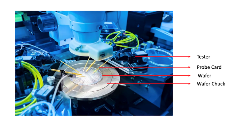
Figure 1: Automatic Test Equipment for Wafer Testing
For new process nodes, it is important to perform wafer testing to save on the packaging cost and provides invaluable feedback to foundries to fine tune the manufacturing process. For mature processes, wafter testing allows design houses to perform wafer-level chip binning that involves sorting the chips into different buckets based on performance and sometimes functionality. The chips exhibiting higher performance or more functionalities can be sold at a premium in contrast to other chips offering lower performance or lesser functionality.
Further reading: What is a ProbeCard?
Package Test: Package Test is the second step of chip production testing which is performed after the wafer is packaged. Package serves many purposes:
Package testing helps ensure the quality and reliability of the final integrated circuit meets the specifications. In addition to assessing the package for possible shorts, open or weak connections, it checks the electrical performance of the IC after packaging, which includes checking signal integrity, power consumption, noise levels. Thermal analysis is another crucial testing performed after packaging to ensure there are no overheating issues due to poor packaging. For mature processes with proven yield, wafer testing is sometimes deemed optional and only package testing is performed.
Estimate NRE for test development and an indicative per-unit test cost.
Further reading: Understanding Semiconductor Testing
