

Imagine launching a groundbreaking smartphone, only to discover that a significant percentage of the devices are faulty, leading to massive recalls, disappointed customers, and financial losses. Or, even graver, consider an autonomous car failing mid-journey due to a chip malfunction, jeopardizing passenger safety. Such scenarios aren’t mere conjectures—they highlight the very real, tangible implications of inadequately tested semiconductors.
Enter the world of semiconductor production testing—a critical phase in the chip production process that ensures your favorite devices work seamlessly. In this guide, we’ll delve deep into the intricacies of semiconductor testing, demystifying its importance and methods.
Fabrication and manufacturing defects are inevitable, particularly for lower technology nodes. Similarly, the presence of functional bugs cannot be ruled out in a fabricated chip.
Chip production testing helps with the following:
ATEs are sophisticated systems designed to perform tests on semiconductor devices, ensuring that the chip functions correctly. Essentially, they simulate real-world scenarios where the chip would be operational, applying various electrical stimuli to the device and subsequently measuring its responses. This procedure not only ensures that the chip meets its functional and performance specifications but also identifies any manufacturing defects or design flaws. The capabilities of ATEs are vast, ranging from high-speed digital tests, mixed-signal tests, power tests, RF tests, to even memory tests. Their precision, combined with rapid testing capabilities, makes them indispensable in the semiconductor manufacturing process. As of my last update in 2021, three leading vendors dominating the ATE landscape are Advantest, Teradyne. Each offers a unique suite of testing solutions, continuously innovating to match the evolving complexities of modern semiconductor devices.
Estimate NRE for test development and an indicative per-unit test cost.
The fabricated parts can be tested before packaging and after packaging. Let us look at these in detail:
Wafer Test: Wafer Test is also referred to as Chip Probe Test, and it is performed on the die itself before chip packaging. It is performed using Automatic Test Equipment which has the tester and the needle like structures called the probe cards to establish electrical contact between the wafer pads and the tester. The tester applies various electric stimuli to the wafer and measure responses from them.
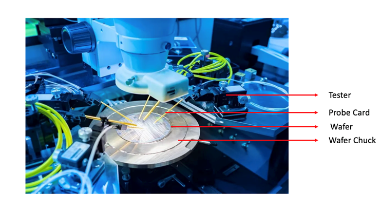
Figure 1: Automatic Test Equipment for Wafer Testing
For new process nodes, it is important to perform wafer testing to save on the packaging cost and provides invaluable feedback to foundries to fine tune the manufacturing process. For mature processes, wafter testing allows design houses to perform wafer-level chip binning that involves sorting the chips into different buckets based on performance and sometimes functionality. The chips exhibiting higher performance or more functionalities can be sold at a premium in contrast to other chips offering lower performance or lesser functionality.
Package Test: Package Test is the second step of chip production testing which is performed after the wafer is packaged. Package serves many purposes:
Package testing helps ensure the quality and reliability of the final integrated circuit meets the specifications. In addition to assessing the package for possible shorts, open or weak connections, it checks the electrical performance of the IC after packaging, which includes checking signal integrity, power consumption, noise levels. Thermal analysis is another crucial testing performed after packaging to ensure there are no overheating issues due to poor packaging. For mature processes with proven yield, wafer testing is sometimes deemed optional and only package testing is performed.
The quality and efficiency of the production process is assessed by metrics of yield and defect level.
Yield is defined as the fraction of functional and error-free chips produced divided by the maximum number of chips that could have been produced on a single wafer.
A new process node often has a low yield to begin with. Foundries strive to improve the design yield by analyzing the defects, improving the process- whether that be with respect to designing and upgrading the equipment or optimizing the use of chemicals, fine tuning the DRC decks to modify the design for better manufacturability, and having a tighter control over the environmental variables.
As a rule of thumb, the center of the wafer usually results in a higher yield in contrast to the edge of the die because the process variations are larger along the edge. This is also referred to as Edge Yield Issue.
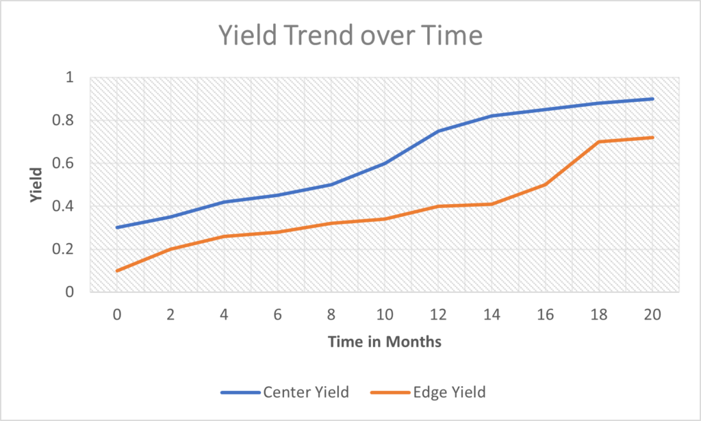
Figure 2: Trends of center yield and edge yield over time.
Many researchers have also recommended excluding all the chips located at the edge of the wafer because the edges are more susceptible to chips, cracks, and identification notches. The probability of photoresists residue material also tends to be higher along the edges. Edge exclusion may reduce the useable area of a wafer by as much as 2%.
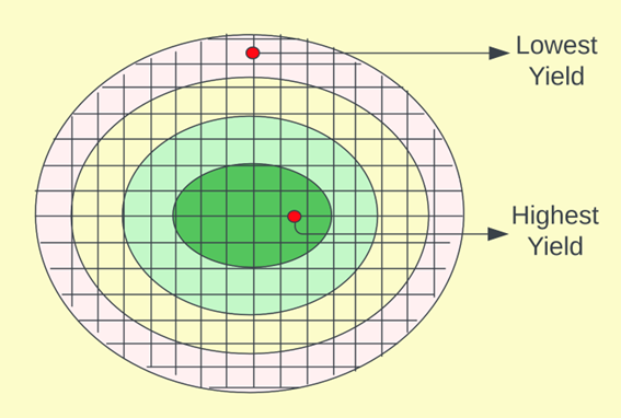
Figure 3: Yield Gradient. The chips along the edge exhibit lower yield.
Another parameter that defines the manufacturing quality of the product is defective parts per million (DPPM). It refers to the maximum number of defective parts shipped for every million parts shipped to the customer. A very low DPPM is extremely critical for semiconductors catering to aerospace, military, medical and automotive applications where a system failure can potentially have a catastrophic impact.
On similar lines, some manufacturers also look at the Defect Density (DD) of the chip which refers to the number of defects per unit chip area. Lower defect density translates into better throughput for customers. Defect density is measured in defects per square centimeter. As a rule of thumb, a defect density below 0.5/sq cm is considered a reasonably good metric. For mature processes, the defect density can be lower.
Next, we will discuss different types of wafer and package tests to conclude this article. All these tests are performed using the Automatic Test Equipment (ATE) that has the capability to apply input signals and monitor output responses to ensure that the device is performing as per the specifications. The tests include:
Scan Testing: Scan Testing is a design for test (DFT) technique used to facilitate the detection of various manufacturing faults in the silicon. Scan tests involve capturing data into a set of flop-flops to observe the chip’s behavior. There are two major flavors of scan testing:
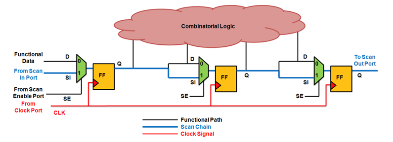
Figure 4: Scan Testing
Power Integrity Tests: Power integrity tests focus on how power is distributed throughout the chip. Some common power integrity tests include:
Signal Integrity Tests: Signal integrity tests assess how signals propagate within and between different parts of the circuit, and focus on maintaining the quality of electrical signals. Signal integrity tests create an “eye diagram” by plotting signal transitions over time which helps in assessing signal quality, jitter and noise margins.
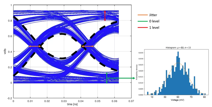
Figure 5: Eye diagram for Signal Integrity Test
Electro-Static Discharge Tests: It is estimated that ESD causes millions of dollars in real losses each layer, and that is the reason it is critical to evaluate the chip’s response to electrostatic discharge events to ensure its robustness against ESD events. Integrated circuits use ESD protection circuitry in the form of ESD clamps that are placed throughout the designs. Electro-static discharge tests ensure that there is a low resistance path to allow a safe electrostatic discharge without harming the internal circuitry of the IC.
Thermal Tests: Thermal tests assesses the chip’s performance and reliability under different temperature conditions to ensure it operates within acceptable thermal limits. It also evaluates how a device or system responds to and manages heat. Thermal testing involves measuring temperature changes, heat dissipation and thermal behavior under various conditions like the workload. This is particularly critical for automotive, aerospace and military applications.
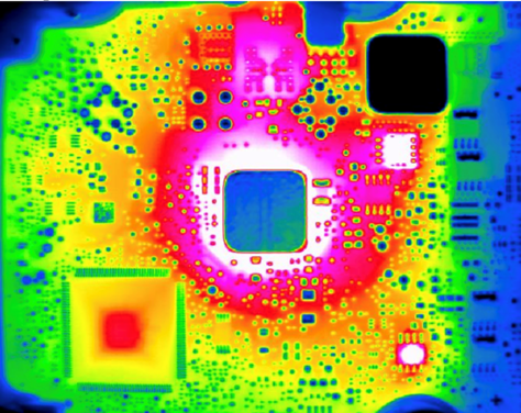
Figure 6: Sample thermal profile of a printed circuit board
Functional Tests: Functional tests assess whether the chip performs its intended functions correctly. This involves applying various inputs and verifying that the outputs match the expected behavior.
Each type of test serves a specific purpose in identifying defects or ensuring specific chip specifications and functionalities. The combination if these tests help ensure the overall quality and reliability of the chips before they are packaged and shipped to customers. The cost of fixing a bug increases exponentially from design phase where it is easiest, fastest, and cheapest to fix a bug to fixing a bug in production where it is most expensive, time consuming and in some cases, prone to lawsuits!
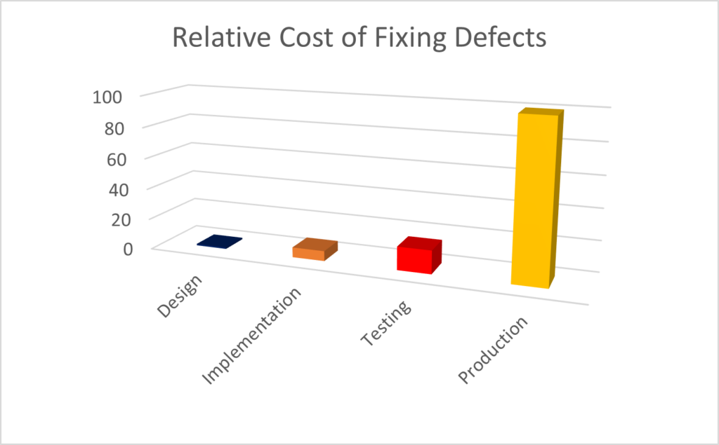
Figure 7: Relative cost of fixing defects increases exponentially from design to production
Further reading: Introduction to LoadBoard Design and Production
Further reading: What is a ProbeCard?
Further reading: A Guide to Semiconductor Wafer Test
Further reading: IC Testing Overview
References:
