

In the realm of cutting-edge electronics, the shift from silicon-based components to gallium nitride (GaN) technology is making waves across industries. As traditional semiconductors reach their performance limits, GaN High Electron Mobility Transistors (HEMTs) offer a compelling alternative with superior efficiency and enhanced thermal management. Whether you’re an engineer diving into modern electronics or a curious enthusiast eager to explore this transformative technology, understanding GaN HEMTs is essential in grasping the future direction of power electronics.
GaN, short for gallium nitride, provides distinct advantages over its silicon predecessors. Characterized by higher efficiency and performance, GaN HEMTs are rapidly becoming indispensable in applications ranging from power electronics to RF and microwave industries. The key differences between GaN and silicon devices not only highlight the advanced features of GaN HEMTs but also emphasize their potential to revolutionize various sectors, including automotive and renewable energy systems.
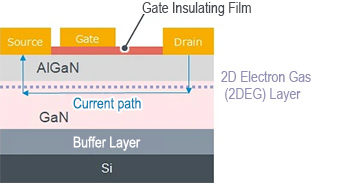
Source: Rohm
Gallium Nitride, or GaN, is transforming the world of electronics. This semiconductor material is known for its exceptional electronic properties, making it ideal for advanced technologies. GaN’s primary role is in power electronics, where its efficiency outshines traditional materials like silicon. With its ability to handle higher power densities and operate at higher frequencies, GaN technology is pushing the boundaries of what is possible in modern devices. From field effect transistors to two-dimensional electron gas applications, GaN continues to be at the forefront of innovation.
What is GaN?
GaN stands for Gallium Nitride. It is a semiconductor material used in electronic devices. Unlike traditional silicon, GaN can operate at much higher voltages and temperatures. This gives it an edge in high-power and high-frequency applications. It’s also known for its high electron mobility, an important trait for speeding up the performance of electronic components. GaN is used in power conversion, high-speed switching, and radio frequency systems. Its efficiency makes it an attractive choice for industries aiming to reduce energy consumption and improve device performance.
Characteristics of GaN HEMTs
GaN High-Electron-Mobility Transistors (HEMTs) are a cornerstone of modern electronics. They offer superior channel mobility due to their two-dimensional electron gas (2DEG) channel. This leads to faster switching speeds and greater efficiency. The breakdown voltage of GaN HEMTs is also higher, making them reliable in high-power settings. A key feature is the p-GaN gate which enhances normally-off operation, ensuring safety in power applications. The barrier layer is crucial for creating a high electric field, which contributes to the power efficiency. Moreover, GaN HEMTs have minimal gate leakage current, reducing energy loss. This results in better overall performance compared to other semiconductor materials.
GaN vs. Silicon: Key Differences
GaN and silicon have unique properties that set them apart. GaN’s primary advantage is in its ability to handle higher power densities and voltage levels. This makes it more suitable for applications that require high power efficiency. GaN also boasts higher electron mobility, allowing for faster electronic response and greater performance in switching devices. In contrast, silicon is more accessible and cost-effective, but it falls short in high-power situations due to its lower breakdown voltage. GaN devices have the edge when it comes to operating with hot electrons, which is crucial for high-speed applications. While silicon remains a staple in many devices due to its availability, GaN is the material of choice where performance is prioritized. GaN’s capacity for handling deep-level traps and reducing gate leaks further highlights its superiority in electric and electronic applications.
Advantages of GaN HEMTs
Gallium Nitride High Electron Mobility Transistors (GaN HEMTs) are revolutionizing the world of electronics. They offer distinct advantages over traditional silicon-based transistors, particularly in power applications. The unique properties of GaN, such as a wider bandgap and high electron mobility, make HEMTs an excellent choice for various uses. These transistors support higher frequencies and voltages, allowing for improved performance in power conversion systems. They have become essential in fields requiring efficient and robust solutions for electronic device management.
Efficiency and Performance
GaN HEMTs significantly enhance efficiency and performance. Their high electron mobility and power densities lead to faster switching speeds, reducing power loss during conversions. By minimizing gate leakage current and enhancing channel mobility, GaN HEMTs ensure efficient use of power. These transistors can operate at higher voltages, which means they handle more power without increasing size. The two-dimensional electron gas (2DEG) channel also contributes to their outstanding performance. These features make GaN HEMTs perfect for high-speed switching, ensuring effective energy use in various applications.
Thermal Management Benefits
One of the key advantages of GaN HEMTs is their thermal management benefits. Due to lower power loss, less heat is produced, which reduces reliance on cooling systems. This leads to cost savings and increased system reliability. Their ability to operate at higher temperatures without degradation extends device longevity. GaN HEMTs also maintain consistent performance, even under thermal stress, due to their robust structure. This capacity allows designers to create more compact systems by reducing the need for large heat sinks or cooling systems, optimizing space and resources.
Reliability and Longevity
The reliability and longevity of GaN HEMTs arise from their robust semiconductor materials. With a breakdown voltage that far exceeds that of silicon transistors, GaN HEMTs can handle higher electric fields without damage. This resilience ensures continued performance in demanding environments. The p-GaN layer and effective use of buffer layers reduce deep-level traps that can degrade devices over time. These features contribute to a normally-off operation, enhancing safety and reliability in electronic circuits. By offering a longer lifespan, GaN HEMTs reduce maintenance needs and costs over the product’s life cycle, providing value over time.
Gallium Nitride High Electron Mobility Transistors, or GaN HEMTs, are transforming various industries with their superior performance. Known for high power densities and efficiency in power conversion, these transistors offer significant advantages over traditional silicon-based technologies. They perform well in both power electronics and radio frequency (RF) applications. The ability of GaN HEMTs to handle high electric fields and improve channel mobility makes them suitable for many cutting-edge applications. From enhancing high-speed switching in power electronics to facilitating robust performance in the RF and microwave sectors, GaN HEMTs continue to gain popularity. This versatile semiconductor technology also finds applications in the automotive sector, driving innovation and efficiency.
Power Electronics
In power electronics, the efficiency and speed of GaN HEMTs are unmatched. Their high breakdown voltage and low gate leakage current make them a preferred choice for power conversion. GaN HEMTs are capable of operating at higher temperatures and voltages compared to their silicon counterparts. This means devices can be smaller and more efficient. Additionally, GaN HEMTs support enhancement mode operations, which are crucial for achieving normally-off operation in electronic systems. The inclusion of a p-GaN gate and field plate further enhances performance. As a result, GaN HEMTs are ideal for applications requiring high-speed switching and efficiency, showcasing their prowess in energy systems.
RF and Microwave Industries
GaN HEMTs are revolutionizing the RF and microwave industries due to their exceptional electron mobility and power densities. Their ability to sustain high-frequency operations makes them suitable for wireless communications and radar systems. The two-dimensional electron gas, or 2DEG channel, in GaN HEMTs provides high electron densities, ensuring optimum performance. Advanced designs, inspired by professionals like Khan et al., often leverage barrier layers and buffer layers to stabilize operations. Such innovations allow GaN HEMTs to deliver better performance by managing hot electrons and enhancing mobility electrons. In this dynamic field, GaN HEMTs are becoming indispensable for robust and reliable RF applications.
Automotive Sector
The automotive sector is also benefiting from GaN HEMTs. These transistors offer high power efficiency, meeting the growing demands for energy-efficient vehicles. Their compact size and high switching speed make them perfect for electric and hybrid vehicles. GaN HEMTs are integrated into field effect transistors to manage power distribution and conversion efficiently. Deep-level traps are minimized, enhancing the reliability and lifespan of automotive systems. As electric vehicles become more mainstream, the need for efficient power electronics grows. GaN HEMTs are at the forefront of this revolution, providing the high-performance standards needed for the future of the automotive industry.
Gallium Nitride (GaN) is a powerful semiconductor material transforming various industries due to its superior properties. Packaging techniques for GaN High Electron Mobility Transistors (HEMTs) are crucial in maximizing their performance. The packaging process impacts the parameters like power densities, breakdown voltage, and efficiency in power conversion. Understanding innovative packaging methods helps in leveraging the full potential of GaN HEMTs.
Enhancing Performance
To optimize the performance of GaN HEMTs, it’s essential to focus on the materials used and the techniques applied during packaging. The use of materials with high thermal conductivity is critical. They help in efficiently dissipating heat, allowing devices to operate at higher power densities and greater efficiency. Additionally, using barrier layers can reduce electric field stress, enhancing device reliability.
Enhancing electron mobility and channel mobility is crucial. This is achieved through innovative designs like the 2DEG channel and p-GaN gate structures, which enable better control and switching speeds. These designs lead to improved performance and efficiency in power conversion, making GaN HEMTs ideal for high-speed switching applications. By incorporating these elements, GaN HEMT packaging can significantly enhance device efficiency and longevity.
Packaging Trends and Advances
The packaging of GaN HEMTs has seen several advancements driven by evolving technology demands. A noteworthy trend is the miniaturization of packages, which aids in reducing parasitic inductances and improving the device’s overall electrical performance. These compact designs also support higher-frequency applications, making them suitable for modern power systems.
Advanced packaging techniques also focus on reducing gate leakage current and managing hot electrons. Using field plates and p-GaN layers, manufacturers can limit these issues, enhancing normally-off operation reliability. Buffer layers and deep-level traps can further mitigate potential damage from electric fields, ensuring device safety and longevity.
The industry continues to innovate with new materials and designs, often inspired by reference designs from experts like Khan et al. These innovations constantly push the boundaries of what GaN HEMTs can achieve, promising a future with even more efficient, reliable, and powerful semiconductor devices. As trends evolve, we can expect GaN packaging to meet emerging needs in energy and technology sectors.
Integrating GaN HEMTs with gate driver ICs is critical for efficient power conversion and high-speed switching. Gate driver ICs ensure the GaN HEMTs operate effectively by providing the correct voltage and current levels to the gate. This integration is vital in applications like electric vehicles and renewable energy systems where power density and savings are critical. Proper integration allows for better control of gate leakage current and the enhancement of overall system performance. This involves understanding the semiconductor materials involved and selecting components that minimize power losses and maximize reliability.
Importance of Gate Drivers
Gate drivers are essential in controlling the switching characteristics of GaN HEMTs. They manage the electric field across the gate and ensure that the enhancement mode is achieved. Without a proper gate driver, the device might not switch at the desired speed, reducing its effectiveness. Moreover, gate drivers help maintain a stable two-dimensional electron gas (2DEG) channel, which is critical for high-speed and efficient operations. Therefore, selecting an effective gate driver can significantly improve efficiency in power conversion and prolong device life by reducing stress on the components.
Compatibility and Selection Criteria
Selecting the right gate driver involves ensuring compatibility with the GaN HEMT’s specific requirements. The gate driver must support normally-off operation, meaning the device is non-conductive in its default state. This is crucial for safety and efficient power use. Consideration must be given to the driver’s ability to handle high electron mobility and maintain a low gate leakage current. The choice also depends on how well it integrates within the existing circuit, addressing issues like breakdown voltage and accommodating deep-level traps. Studying the GaN HEMT’s band diagram can offer insights into the correct gate electrode and p-GaN layer thickness needed for optimal integration. Ensuring these criteria are met will lead to reliable and high-performing electronic systems.


