

Gallium Nitride (GaN) technology is a cutting-edge semiconductor material that is revolutionizing the electronics industry. With its superior performance and durability, GaN is enabling the development of more efficient and powerful devices, such as smartphones, laptops, and LED lights. By leveraging the unique properties of GaN, companies can create innovative solutions for a wide range of applications and industries. Discover the benefits of GaN technology and how it is shaping the future of electronics.
Gallium Nitride is the member of group III-V nitrides and it is the second most important semiconductor material after silicon (Si). GaN has low power loss and high switching capability and finds its use mostly in RF applications. GaN has wider bandgap (WBG) ranging from 3.49s to 6.2eV which results in large breakdown voltages. The wider bandgap is due to the relatively large bonding energy of the atomic components in its crystaline structure. Thus with wider bandgap, it has low dielectric constants with high thermal conductivity pathways. Also, it is also suitable for high temperature applications.
Table 1 depicts the different parameters and their values for GaN semiconductor material [1]. GaN possess hexagonal symmetry which makes it different from Gallium Arsenide (GaAs) and other Silicon (Si) based devices. This hexagonal structure results in spontaneous and piezoelectric polarization in GaN. There is a rapid progress in GaN devices because of the advanced improvement in contact technology and material quality. GaN and its alloys have the potential to design high power electronic devices like transistors and thyristors. These devices include blue-green lasers, blue-green LEDs, Ultraviolet (UV) and GaN Heterostructure Field Effective Transistors (HEFTs). GaN devices have low input and output capacitance and low on-resistance. It is also used for designing the luminance devices and colored displays for cell phones.
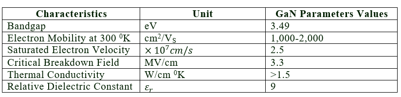
Table 1: GaN Parameters and their values
The development in technology of the nitride group emerged in last two decades of 20th century although Pankove in 1971, had already demonstrated GaN-based LED. In early 1990’s, the major properties that made GaN material an attractive next generation semiconductor material were its wider bandgap, high electron mobility and saturated electron velocity. It was supposed to be an excellent semiconductor material for high frequency and high power transistors. The lack of bulk sources of GaN led to its growth on substrates like Si, SiC and Sapphire. In fact, Sapphire is the most commonly used substrate for deposition of GaN as it has hexagonal structure and possess good thermal stability. The pace for the GaN technology for electronics and optoelectronics applications was controlled by the fundamental development of material. Table 2 gives the historical background of GaN devices [2].
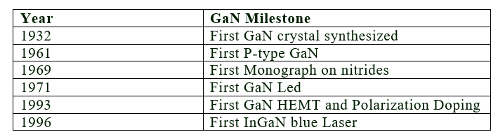
Table 2: Historical background of GaN devices
In 2004, Eudyna Corporation in Japan introduced first GaN HEMT (High Electron Mobility Transistors) based devices with depletion mode radio frequency transistors. [3] The structure of HEMT was based on the phenomenon that was first described by Mimura et al in 1075 and then by khan et al in 1994. Nitronex Corporation in 2005 by using their SIGANTIC technology introduced first depletion mode RF HEMT devices made with GaN grown on Si wafers. Hence several companies entered in the market of designing RF applications using GaN RF transistors. These transistors did not find their usability much for other applications because of the device cost and their ability to operate in depletion mode (as they needed negative voltages at gate terminal for turning OFF).
In 2009, eGaNFETs (enhancement mode GaN grown on Silicon field effect transistors) were introduced as power MOFSET (metals oxide semiconductor field-effect transistor) replacement as they do not need negative voltages for turning them OFF) by EPC (Efficient Power Conversion Corporation). Since then many companies, like Panasonic, GaN Systems, TSMC, ON Semiconductor, and Transphorm have shown their interest to manufacture GaN transistors for power conversion market. So GaN can be considered as a dominant candidate for next generation power transistors.
Figure 1 depicts the summary of features and the associated benefits offered by GaN devices. GaN devices are used for defense systems since it offers significant advantages over existing Si, GaAs, and vacuum electronic device based amplifiers. These advantages include high voltage and broadband performance with high drain efficiency.
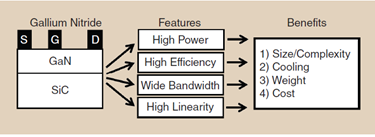
Figure 1: Summary of features and benefits of GaN RF power [4]
Saturation velocity of GaN material is higher than casual semiconductor materials which is because of large energy separation of electrons between the conduction band valleys.
GaN based devices are expected to improve the conversion efficiency in traditional power systems. The motivation behind is to reduce the resistance loss by shortening the space between anode and cathode keeping even high blocking voltages.
GaN can now provide high efficiency with wider bandwidth and linear power for next generation data systems because of alternate technology optimizations. Hence increased linear power from a single GaN has resulted in weight and size reduction. With maturity of technology, system designers are trying to balance the performance benefits. Data sets continue to develop for different applications of GaN in different market places. Researchers are being more focused on its usability with high performance rate and highlighting advancement in reliability by addressing the fundamental material issues systematically.
Although GaN based HEFTs have achieved output power of 30W/mm at the frequency of 10GHz which makes them suitable for different microwave applications. But still there are some problems to be solved like: gate leakage, poor reliability, and current collapse in such devices.
GaN devices have not yet achieved the power performance equivalent to SiC or Si because of the problems related to substrate. Also only 2’’ diameter of GaN wafer has been achieved so far at the cost of 10 times higher than SiC and up to the cost of 100 times than simple Silicon [5]. That’s why GaN is deposited on these substrates. But this leads to defects because of difference in crystalline structures of both materials.
GaN based power devices possess low stored charge and small capacitances but these devices experience high switching stresses. This may result in serious switching limitations especially in high frequency power converters. The presence of high density of crystal defect in SiC and GaN may even worsen this problem that may result in poor field reliability. In order to optimize field reliability and performance, specific guidelines for device selection are needed. [6]
Owing to wide bandgap and chemical stability of GaN, different challenges are there to be tackled in order to make these devices more useful from commercial perspectives. The challenges include: poor p-type doping, need of high temperatures for implant activation, dry etch damage, low dry etch rate and low selectivity over etching masks [7]. In order to fully exploit the device advantages, a number of critical advances are required in the areas of implantation doping and isolation, etching process of device, and low resistive ohmic contact to p-type material.
Ultra Violet (UV) LEDs based on GaN will find their applications in purification of water and air, sterilization of food, fire detection, detection of bio-agents, and in biomedical systems. UV based LEDs use GaN that is grown either on SiC or sapphire substrate and rely on the emission through sapphire rather than that of SiC. Because of its improved efficiency, GaN HEMT has already been widely used for 4G/LTE base station amplifiers. Both the large MIMO amplifiers and the macro cell have the potential for further efficiency improvement. Devices like GaN HEMTs are desirable for 5G base station applications.
Let us consider an application of wireless power transfer (WPT) that can be enabled using GaN based single phase converters. Generally in WPT applications, Si based or SiGe-based RF MOSFETs are used. WPT systems are rated at low power applications in RF fields because of high current stress of resonance tank and limited device ratings. High power (~10KW) WPT converters have been enabled by GaN.
Two different approaches for designing the transmitter side using GaN based devices are shown in the Figure 2.
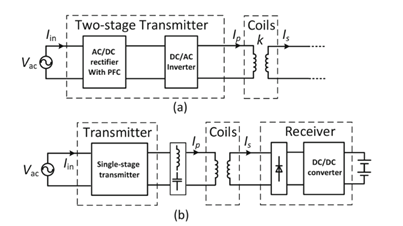
Figure 2: Wireless Power Transmitter Circuit
The first approach (a) of two stage transmitter of 6.78MHz consists of AC/DC rectifier with power factor correction provides input to ZVS (zero voltage switching) tank assisted full bridge inverter. Power efficiencies obtained by rectifier and inverter in this scheme are 98.6% and 93% respectively at 100W full load. While overall efficiency obtained in this topology is 91.7%.
The other scheme (b) combines two stage by eliminating one phase leg and operating the rectifier in discontinuous conduction mode totem-pole PFC mode. This gives efficiency (approximately equal to 92.1%) slightly greater than two-stage transmitter with less number of components that can be optimized further. Thus we can say that GaN inverters can improve the conventional converters efficiencies of WPT systems that are typically around 50% ~ 70%.
Dense Power Integration in DC-DC Converters
Wide power range applications like power factor correction and renewable energy utilization use DC-DC converters topology as shown in Figure 3. When the transistor Q1 is turned ON, inductor is charged through the input voltage source which is PV panel in this case. Diode D1 is reverse biased during this time. Freewheeling diode is used as a reverse recovery diode which avoids the voltage spikes at the drain of Q1. When Q1 is turned off, capacitor C1 is charged through the PV Panels as well as the energy stored in the inductor.
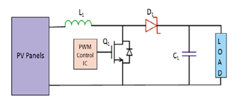
Figure 3: Dense Power Integration in DC-DC Converters
In the absence of solar power, appropriate arrangements must be made in order to operate this circuit in the boost mode. There is an inverse relation between the frequency and the sizes of capacitors and magnetic components. Hence for reducing converter size and cost, we need high switching frequency. This switching frequency can be kept high (>1MHz) using GaN based power transistors as compared to MOSFETs, while maintaining low conduction power losses. High switching frequency reduces inductor and capacitors sizes exponentially as shown in the graph of Figure 4. Thus DC-DC converters can be made more compact and can facilitate dense power integration using GaN based devices.
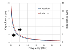
Figure 4: Relation Between the size of magnetic and capacitive components and frequency
Here is a list of 10 Gallium Nitride applications:
Answer a few questions and get a recommended shortlist of foundries. Full scoring and a longer shortlist by email.
3-Stacked GaN HEMT Monolithic Microwave Integrated Circuit (MMIC) Chip
Figure 2 depicts the schematic of 3-stacked GaN HEMT MMIC chip. It can be noticed that three GaN HEMT devices are connected in cascaded manner. There is an addition of two more bias terminals than the normal drain and gate bias. These are the floating point bias between first and second transistor and between second and third transistor.
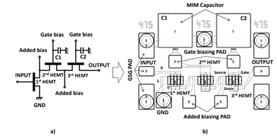
Figure 5: 3-Stacked GaN HEMT topology
In this way we can control the bias condition for each transistors individually. By using metal-insulator-metal (MIM) technology two RF-bypass capacitors are realized. While for chip evaluation, input and output terminals are ground-single-ground (GSG) connection. Metal transmission lines are used for interconnections inside the MMIC. The MMIC chip size is equal to 674𝜇m×1025𝜇m
674μm×1025μm [8]674𝜇m×1025𝜇m [8]
.
Here is the list of names and links of companies that manufacture GaN wafers:
DB HiTek
[1] https://ieeexplore.ieee.org/document/6492190/
[2] https://ieeexplore.ieee.org/document/1504293
[4] J. B. Shealy, R. Vetury, B. Trabert, and D. W. Runton, “A manufacturable, high power RF gallium nitride (GaN) technology portfolio with 65 V operation and enhanced linearity,” in Proc. IEEE Int. Conf. Microwaves, Communications, Antennas Electronics Systems, 2011, pp. 1–8.
[5] N. Kaminski and O. Hilt, “SiC and GaN devices – wide bandgap is not all the same,” IET Circuits, Devices & Systems, vol. 8, no. 3, pp. 227–236, may 2014.
[6] https://ieeexplore.ieee.org/document/6645319/
[7]https://books.google.com.pk/books?id=onrSAOv1u8AC&printsec=frontcover&dq=drawback+of+Gallium+nitride&hl=en&sa=X&ved=2ahUKEwjevqqmus77AhWOSKQEHf5QBUk4ChDoAXoECAkQAg#v=onepage&q=drawback%20of%20Gallium%20nitride&f=false
[8]https://books.google.com.pk/books?id=D2gKEAAAQBAJ&pg=PA96&dq=chips+that+use+GaN&hl=en&sa=X&ved=2ahUKEwjui8mS9OX7AhWqZaQEHTUvA88Q6AF6BAgJEAI#v=onepage&q=chips%20that%20use%20GaN&f=false


