

An Integrated Circuit (IC), also called a chip or a microchip is a set of electronic circuits on a single small flat piece (or “chip”) of semiconductor material, usually silicon. Modern ICs are very complex and contain millions of transistors on a single chip.
Based on their design methodology, flexibility, and applications there are different types of ICs:
Since the focus of this article are ASICs, we will divide them into two groups: ASICs and non-ASICs. We will discuss here ASICs and their types.
Application Specific Integrated Circuit (ASIC) is a non-standard integrated circuit designed for a specific use or application. ASIC is usually designed for a product that will have a large production run, and it contains a huge part of the electronics needed on a single integrated circuit. The cost of an ASIC design (e.g. NRE) as a result is very high, and therefore ASICs are usually used for high volume products.
Even though ASIC’s design cost is quite high, it can be cost effective for many high-volume applications, especially when a significant part of a huge system can be integrated into one ASIC circuit, significantly decreasing the number of external components. ASIC helped to revolutionized technology by reducing the size of electronic products and increasing the density of logic gates per chip. Few examples of ASIC can be Intel’s CPU or a bitcoin ASIC. There are two main methods of ASIC design:
Semi-custom design itself is divided into few groups. The classification of ASICs is shown in the Figure 1 below:
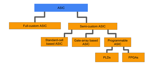
Figure 1 – Types of ASICs
Sometimes Programmable ASICs are considered separate from Semi custom ASICs. There is another classification of ASICs, not so different which is shown below:
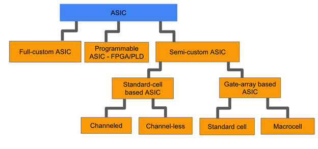
Figure 2 – Classification of ASIC chips
Now let’s briefly discuss the different types of ASICs.
In case of full-custom ASICs some or sometimes all mask layers are customized. It takes usually 8 weeks to manufacture this type of ASIC (of course, this does not include the design time).
Full-custom ASICs are needed only when:
Full custom ASICs have the following advantages:
Of course, they also have disadvantages some of which are shown below:
The design flow off Full-custom layout from schematic are shown in the figure 3 below:
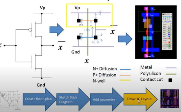
Figure 3 – The layout design flow for full-custom ASIC
First group of Semi-Custom ASICs are Standard-Cell based ASICs (CBICs) that are using pre designed logic cells called standard cells. When we say ASIC we usually understand this type of ASICs because they are the most common. For creating this type of ASICs logic cells are used from:
The layout of NAND2X1 standard cell is shown in the Figure 4.
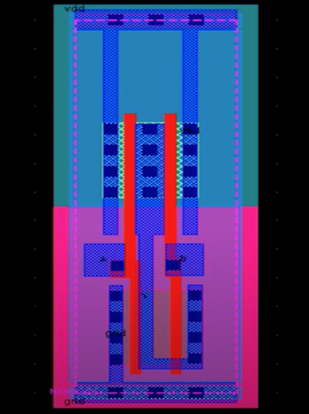
Figure 4 – NAND2X1 standard cell layout
Standard cells of library used in Semi-custom Standard-Cell based ASIC design are constructed using full-custom design methodology. They ensure the same performance and flexibility but reduce time and risk. Thus, ASIC designer defines only placement of standard cells during the design of S Standard-Cell based ASICs.
The construction of flexible blocks in CBIC is done by the following principles:
In this type of Semi-Custom ASICs (CBIC) all mask layers (transistors and interconnect) are customized. Manufacturing process usually takes 8 weeks. In this type of ASICs custom blocks can be embedded. As other types of ASICs they have both advantages and disadvantages. Some of the advantages are shown below:
Some of the disadvantages of this type of ASICs are:
In a gate array based ASIC, transistors are designed and fabricated on a silicon wafer, but interconnects are not fabricated. Base array is a predefined pattern of transistors on a gate array.
The smallest element that is repeated to forma gate array is called base cell. Only the top few layers of metal interconnects that define the interconnect between transistors, can be defined by the designer using custom masks. This is usually called a masked gate array (MGA). This type of ASIC has less turnaround time: usually from few days to couple of weeks.
A gate array, masked gate array or pre-defined gate array uses books (macros) to decrease turnaround time and comprises a base array made from. A primitive cell or a base cell. There are three types of gate arrays:
In the channeled gate array only, the interconnect is customized and uses pre-defined spaces between rows of base cells. Manufacturing lead time takes between 2 days to two weeks. This is very similar to CBIC, but compared to CBIC the space here is fixed.
In channelless gate array, also called channel free gate array, sea-of-gates array or SOG array only some (the top few) mask layers (interconnect) are customized. Manufacturing lead time takes between 2 days to two weeks. The high level architecture of channeled gate array ASIC is shown in Figure 5:
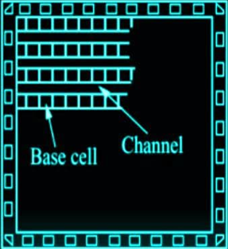
Figure 5 -Architecture of a Channeled gate array ASIC
The biggest advantage of channeled gate arrays is the existence of a pecific space for interconnection.
The biggest disadvantage of this type of arrays is that for example compared to CBIC space is not possible to adjust.
The key differences between a channelless gate array and channeled gate array:
The high-level architecture of this type of ASIC is shown in the Figure 6:
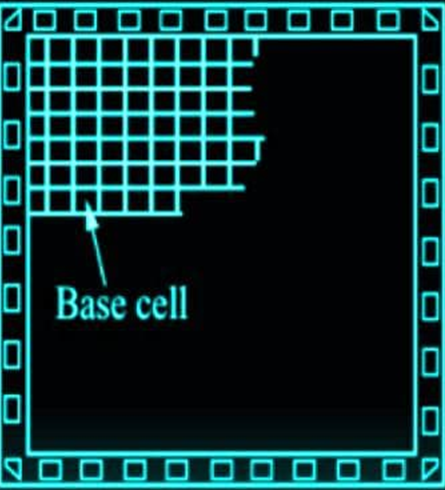
Figure 6 – Architecture of a channelless gate array ASIC
The advantages of channelless gate arrays is that:
The main disadvantages are:
A structured gate array combines some of the features of CBICs and MGAs.
One of the biggest disadvantages of the MGA is the fixed gate-array base cell. This makes the implementation of memory, for example, inefficient or difficult.
In a structured gate array, also called embedded gate array, masterslice or masterimage only the interconnect is customized, custom blocks (the same for each design) can be embedded and manufacturing can take from two days to two weeks.
In an embedded gate array some of the IC area is set aside and dedicated to a specific function.
This embedded area can contain:
The high level architecture of structured gate array ASICs is shown in the Figure 7:
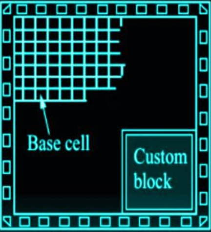
Figure 7- Architecture of a structured gate array ASIC
The main advantages of structured gate arrays are:
The biggest disadvantage is that the embedded function is fixed.
Programable ASICs are type of an ASIC that can be programmed in a hardware level after being manufactured. Some of the programmable ASICs are:
PLDs – They low-density devices that contain 1k – 10 k gates only
FPGAs (CPLDs or FPLDs) are programmable ASICs that combine architecture of gate arrays with programmability of PLDs. PLDs have no customized mask layers or logic cells as a result fast design turnaround. PLDs can be configured or programmed to create a part customized to a specific application.
Some examples of PLD are ROM, PROM, EPROM.
Compared to PLD, FPGA is much larger and can be used for more complex applications. The architecture of an FPGA IC is shown in the Figure 8:
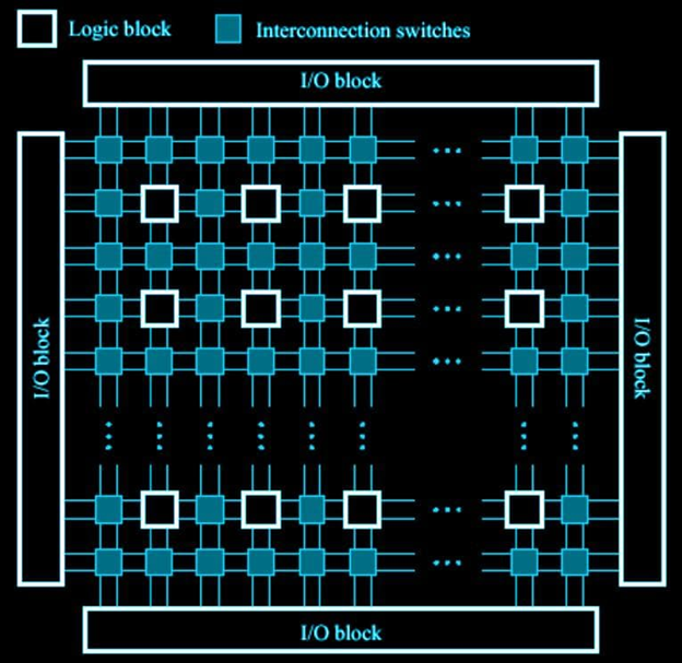
Figure 8 – The architecture of FPGA
Here are some of the main features of FPGA:
One can decide whether or not to use FPGA based on the following factors:
Want to know more?
What is a System on Chip (SoC)
The Smart Guide to Developing an ASIC


