

Consumer electronics markets, the mobile phone market in particular, are extremely demanding. They are driven by the desire to pack more and more functionality and enhanced value into the same size handheld device, and often at lower costs. This drive towards smaller, cheaper and thinner consumer electronics has driven the development of highly integrated electronics and stimulated the development of smaller, thinner packages to compliment this advanced technology. This has led to the development of various wafer bumping packaging technologies by leading OSAT companies and semiconductor foundries.
The assembly of a die in package has followed an evolutionary trend, which started with wire bonding the chip into a relatively large package and is now moving towards eliminating the package altogether either by Chip On Board (COB) or even embedding the die into the PCB.
An important step on this path was to eliminate the wire bonds and replace them with bumps. Wafer Bumping can be considered as a step in wafer processing where solder spheres are attached to the chip I/O pads before the wafer is diced into individual chips. The bumped dies can then be placed into packages or soldered directly to the PCB, i.e. the COB mentioned earlier.
The advantages are many; lower inductance, better electrical performance, higher current carrying capacity, a potentially much smaller footprint and lower cost.
The bumps are typically placed onto an under bump metallisation (UBM) material that is plated onto the die pads.
The bumps are composed of many different materials, defined by the application and use; lead free bumps (SnAg) are common for most applications, though copper pillar bumps offer the advantage of higher density.
With regards to packaged bumped dies, there are several package types available in the industry today:
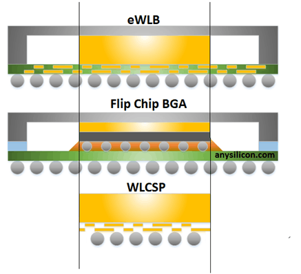
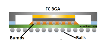
Ball Grid Array (BGA) flip chip packages are still the most common type of package used with bumped dies; the bumped die is attached (flipped) onto a substrate in the package that routes the signals to the package balls. Advantages are good thermal performance and scalability for physically large and complex dies. Low cost FCBGAs use a laminate (PCB type) substrate; build-up substrates are also available that offer finer pitch routing, enhanced signal and thermal performance, and a lower profile, at a cost. A FCBGA is the preferred flipchip solution for high power designs and designs with a large number of balls (over 100, for example).
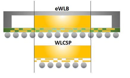
Wafer Level Chip Scale Package (WLCSP) is truly a chip scale package because it’s essentially a die sized package with bumps that are essentially balls that can be soldered directly to a PCB. There are two main versions; one where balls are attached directly to the die pad openings (this, incidentally, gives the shortest path from die circuit to PCB, so achieves optimum signal performance, lowest inductance, highest speed); and another where a Redistribution Layer (RDL) is used to route the chip pad openings (for example from the edges of the die) to balls that can form a regular array across the die – this is referred to as Fan In. In its final form the WLCSP package is the same size as the die. The RDL may be aluminium (Al), copper (Cu) or a combination of aluminium and copper (AlCu). The back side of the die can be left exposed, plated with metal or some protective layer. This is a preferred solution for low-power, low ball count devices where the small form factor is an advantage,
eWLB, or Embedded Wafer Level BGA, is a packaging technology that was introduced in 2009 by ST and STATS ChipPac. It is similar to the WLCSP described above, however the wafers are first diced, the dies spaced apart and a resin material is flowed over the dies then hardened to form a re-constituted wafer. This assembly is referred to as a Fan Out assembly because the relatively small pitch die pads are able to be routed out (fanned out) to a larger pitch array of balls. Multiple RDL levels can be used for complex routing of many pads. The RDL lines are separate by repassivation layers applied in a manner similar to wafer process back-end passivation.
The redistribution layer (RDL) technology plays a crucial role in wafer-level packaging processes to optimize signal wiring and transmission paths between bare dies and solder balls. By adding one or more layers of lateral connections to the original wafer, RDL helps maximize the signal interconnection density and overall flexibility of the product. The RDL technology also involves the use of dielectric materials to protect the RDL layer, acting as a stress buffer, and to ensure the proper functioning of the Under Bump Metallurgy (UBM) technology, which supports the contact pad, solder ball, RDL, and dielectric. Additionally, RDL is a key enabling technology for advanced fan-out wafer level technologies like embedded Wafer Level Ball Grid Array (eWLB), fan-in Wafer Level Chip Scale Packaging (WLCSP), Integrated Passive Devices (IPD), and System-in-Package (SiP) solutions.
![]()
Copper (Cu) pillars are a type of interconnect technology commonly used in advanced wafer-level packaging processes. These pillars are typically made of copper and serve as the vertical connections between different layers of the package. Cu pillars play a crucial role in ensuring the reliability and performance of the package, especially in high-density applications where space is limited. By using Cu pillars, designers can achieve higher signal interconnection density and overall flexibility in the product. Additionally, Cu pillars provide excellent electrical and thermal conductivity, making them ideal for applications that require high-speed data transmission and efficient heat dissipation. Overall, Cu pillars are an essential component in modern wafer-level packaging technologies, enabling the development of more compact and powerful electronic devices.
The process of creating Cu pillar bumps involves depositing copper onto the bond pads of a silicon wafer using electroplating or sputtering techniques. The pillars are then often planarized to ensure a uniform height. A thin layer of solder is then applied to the top of the copper pillars, typically through electroplating or solder paste printing. During the assembly process, the solder on the Cu pillars is reflowed to create a reliable metallurgical bond with the substrate.
SnAg bumping refers to a solder bumping technology used in semiconductor packaging, where a solder alloy composed primarily of tin (Sn) and silver (Ag) is used to create the bumps that serve as electrical and mechanical connections between a chip and a substrate or another chip. The SnAg alloy is popular due to its improved mechanical strength, better creep resistance, and enhanced thermal fatigue performance compared to pure tin solder. These characteristics are crucial for ensuring the reliability of electronic devices, especially in demanding environments.
The process of SnAg bumping typically involves depositing the SnAg alloy onto the bond pads of a silicon wafer using various methods such as electroplating, solder paste printing, or evaporation. After deposition, the solder bumps are often reflowed to create a uniform shape and improve the metallurgical bond with the underlying pad.
The wafer bumping process involves several steps to create the metal bumps on the wafer for interconnecting the IC signal contacts. The steps involved in wafer bumping are as follows:
Wafer bumping is an advanced manufacturing process in semiconductor packaging where metal solder balls or bumps are formed on the wafer before it is diced into individual chips. These bumps serve as the interconnection between the die and a substrate or printed circuit board in a device, providing electrical, mechanical, and thermal performance advantages. Wafer bumping technology, which includes various bump alloys and processes, is essential for flip chip and board-level semiconductor packaging applications.
Wafer bumping services play a crucial role in the semiconductor packaging industry, companies that provide wafer bumping services offer expertise in a range of bump alloys and processes, including printed bump, ball drop, and plated technology with various solder compositions such as eutectic, lead-free, high lead, or copper pillar alloys. These companies typically offer wafer bumping for different wafer sizes, such as 200mm and 300mm, to cater to the diverse requirements of advanced flip chip and wafer level packaging solutions.
Get an indicative packaging cost range, then a detailed breakdown by email.
