

The factors affecting silicon wafer cost are numerous. From the resistivity required for different applications to the physical size of the wafers, and not least the quality grades that separate the pristine from the less perfect; each aspect intricately influences the cost.
As we embark on this explanation, we’ll unwrap the intricacies of demand and pricing in the silicon wafer market, explore how the semiconductor industry’s growth impacts costs, and probe into the manufacturing processes that can sway the expenses one way or another. Understanding silicon wafer cost is not just about numbers, but also about the technological ballet that manufactures tomorrow’s innovations.
Silicon wafer cost is determined by a few factors:
All the above factors are considered when a semiconductor foundry provide you with a price offer.
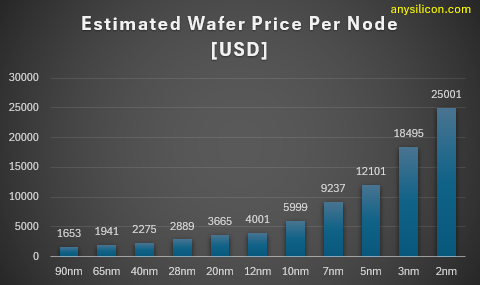
The table below shows the estimated 12″ wafer price per node, with pre defined configuration.
In the competitive realm of semiconductor manufacturing, understanding the intricacies of silicon wafer costs is paramount. A silicon wafer, the substrate for most semiconductor devices, incurs expense through its journey from sand to a sophisticated electronic enabler. Multiple variables interplay to dictate the final price of these essential components, with important cost determinants being processing equipment, wafer size, production volumes, labor costs, and technology node or “nm technology”. The manufacturing process demarcates into various process steps—each incrementing the price through the use of materials, resources, and human expertise.
Silicon wafer prices also vary with the fluctuations in the semiconductor industry, heavily influenced by the electronics industry’s demand. A key factor in cost management is wafer yield, which signifies the number of functioning integrated circuits on a wafer post production. Higher yields lower the cost per chip since more sellable products are realized from a single wafer. Chip size and design rules, reflecting the size and spacing of circuit elements, further mold the economic dynamics. Larger chip sizes tend to reduce yield, thereby amplifying costs, while stricter design rules augment the required processing precision, and hence, the price.
As technology advances, the processing steps become more elaborate due to the need for precision at the nm technology level, demanded by modern electronics. The sophisticated equipment needed for such detailing trails along with an uptick in investment and operational expenses. Another salient consideration is the doping type, where the introduction of specific impurities adjusts the resistivity of silicon to fulfill precise electronic applications, inherently affecting cost. Finally, production volumes play an economic tug-of-war—higher volumes usually mean economies of scale and lower cost per wafer.
In essence, blank silicon wafer cost is a product of numerous factors, ranging from the base material to the complexities imbued during wafer fabrication. Let’s delve deeper into specific aspects that shape silicon wafer costs, namely resistivity, wafer sizes, and quality grades.
Resistivity is a fundamental property of silicon wafers, impacting their applicability and thus, cost. It is a measure of how strongly a material opposes the flow of electric current, and in the context of semiconductors, it is pivotal for determining the performance characteristics of the end devices. Wafers are available in varying resistivity levels tailored to different applications. High-resistivity silicon, essential for radio frequency (RF) and high-power devices, typically commands a premium due to the added complexity in manufacturing processes.
The manipulation of resistivity is carried out through the doping process, where atoms like phosphorus or boron are introduced into the silicon lattice. The precise control of this doping confers specific electrical properties to the wafer, this specificity translating to added costs. For applications requiring ultra-pure, intrinsic (undoped) silicon, the challenge in attaining the required purity level further elevates the price.
Wafer size is a primary influencer of production efficiency in the semiconductor industry. Historically, the industry has transitioned through numerous standard wafer sizes – from the early days of 2-inch wafers to the contemporary 300 mm (12-inch) and even proposals of 450 mm (18-inch) diameters. Larger wafer sizes theoretically allow more chips to be manufactured at once, enhancing the throughput and potentially decreasing the cost per chip. However, the transition to larger wafer sizes mandates significant capital investment in new processing equipment and facilities, which then feeds back into the cost structure.
Moreover, the push for larger wafer sizes intersects with the challenges in maintaining the required level of precision over a larger surface area, offsetting some of the theoretical cost savings with material and process complexities. For instance, handling and processing 300 mm wafers demand more sophisticated, and hence costlier, equipment than with smaller diameters such as the 200 mm wafers. This means that even blank silicon wafer costs can rise substantially as the industry adopts progressively larger standards.
Quality grades in the semiconductor wafer industry are indicative of the purity and crystal defect levels in the silicon. Prime wafers represent the highest quality, offering the best performance for high-end applications, followed by test and mechanical grade wafers which find a place in less critical roles. Prime wafers fetch a higher price point due to their extensive manufacturing process that ensures minimal defects and optimum electrical properties. Conversely, mechanical grade wafers, often used for equipment testing or educational purposes, are less expensive as they do not need to adhere to the stringent specifications demanded by electronic-grade silicon.
End-to-end production in a wafer fabrication facility entails a meticulous assessment of quality at each step, influencing both yield rates and end-product reliability. The nature and stringency of these quality control processes exert a profound impact on the final cost of a silicon wafer. The imperatives of purity and defect management become ever more pronounced with decreasing chip size and the move toward more intricate design rules, which inherently raise the wafer costs and thus, the value proposition of adherence to strict quality grades.
In summary, silicon wafer cost is governed by a complex set of variables including the resistivity tailored for specific applications, the sizes that determine the processing scope, and the quality grades which gatekeep performance standards. Optimizing costs while maintaining the requisite specifications is an ongoing challenge for the semiconductor industry, underpinning the continuous strive for innovation in both materials science and manufacturing processes.
—
In the fast-paced world of semiconductors, the demand for silicon wafers is intricately linked to their pricing. As critical substrates for integrated circuits, their prominence in technology cannot be overstated. Chronicled advances in smartphone technology, cloud computing, artificial intelligence, and the Internet of Things (IoT) are driving an insatiable appetite for silicon wafers. The complexity of manufacturing and the variety of wafers needed also feed into the economics, adjusting the balance of supply and cost. As demand swings, pricing follows suit, reacting to the delicate balance of industry capacity and consumer need.
Silicon wafers lie at the heart of progress in the semiconductor industry. The growing necessity for more powerful and efficient electronic devices catalyzes the increase in demand for higher-grade, larger-sized, and more precisely fabricated silicon wafers. Surging sectors, including electric vehicles, renewable energy, and 5G technology, contribute substantially to the expanding appetite for these wafers. As industries innovate and expand, the requirement for better-performing chips encapsulated in these wafers inflates correspondingly.
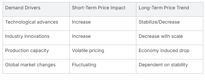
Trends Impacting Demand:
The advent of smart cities and automated factories also factors into the burgeoning demand, necessitating a steady and reliable supply of high-quality silicon wafers.
The impact of escalating demand for silicon wafers on their prices is multifaceted. On one hand, manufacturers scramble to increase production capacity, which can initially increase costs due to investments in state-of-the-art processing equipment and scaling of operations. On the other hand, advances in manufacturing efficiency and economies of scale can eventually lead to a reduction in costs. The following aspects illuminate how wafer prices are affected:
The price trajectory is complex, often demonstrating a counterintuitive trend where heightened demand leads to initially higher prices that may stabilize or decrease over time as the industry adjusts and scales up production efficiencies.
Wafer Demands and Price Fluctuations: A Snapshot
Undeniably, the demand profile for silicon wafers is a potent force in their market valuation. Manufacturers and industry players continuously strategize to strike a profitable balance between cost efficiencies and the burgeoning global demand.
The semiconductor industry sits at the very heart of the modern world’s technological advancement, producing the essential components that power everything from smartphones to supercomputers. Central to this industry are silicon wafers – thin slices of semiconductor material on which microcircuits are imprinted through sophisticated fabrication processes. The costs associated with producing this foundational element can significantly influence the broader economics of the electronics industry.
Two primary cost drivers are the raw materials and the intricate manufacturing process steps that transform a blank silicon wafer into a bed for complex integrated circuits. These steps include photolithography, etching, doping, and many other specialized procedures, each requiring precise control and expensive processing equipment. Moreover, the race to shrink chip size while adhering to meticulous design rules and pushing nm technology boundaries requires constant capital investment, inevitably augmenting wafer costs.
Another cost variable is the size of the wafers themselves; larger wafers provide more surface area, meaning more chips per wafer and potentially reducing the price per chip. However, the transition to larger wafer sizes demands significant overhauls in manufacturing lines and can temporarily spike wafer costs due to increased capital expenditures for retooling wafer fabrication facilities.
In essence, semiconductor wafer costs are an amalgamation of production volumes, labor costs, equipment sophistication, and the relentless innovation that dictates the pace of the semiconductor industry.
Mirroring the ceaseless pace of innovation, the semiconductor industry has grown exponentially. It has evolved from producing simple transistors to crafting highly complex integrated circuits embedded in every facet of modern electronics. This surge is driven not only by the ever-growing consumer electronics market but also by the advent of new technologies and applications.
The growth can be charted across various segments:
Each leap in these sectors propels the need for advanced silicon wafers, cementing the semiconductor industry’s role as a critical engine for global technological progression.
The reverberations of the semiconductor industry’s growth naturally extend to silicon wafer prices. As the demand intensifies and the push for smaller, more efficient chips persists, the cost of manufacturing these wafers experiences pressure from several quarters:
Silicon wafer costs, thus, hinge on a sophisticated interplay of market forces, manufacturing prowess, and global demand. Manufacturers must navigate these variables keenly while also gauging how shifts in wafer size, process steps, and semiconductor industry trends might translate into cost implications for both prime wafers and the further reaches of the wafer market.
In sum, the trajectory of silicon wafer costs is a balancing act, responding dynamically to the semiconductor industry’s continuous advances and the electronic industry’s ever-changing demands. As a key factor in the production of integrated circuits, these costs are a critical heat gauge for the temperature of our tech-driven world.
The semiconductor industry is perennially working towards cost-effective manufacturing methods without compromising on the quality and performance of silicon wafers. One central theme is managing the delicate interplay between wafer yield, chip size, and the cost of production. Increasing wafer size, for instance, can lead to economies of scale but also requires an initial surge in investment and might involve a higher risk of defects affecting larger batches of integrated circuits. Furthermore, doping type—a process to modify electrical properties of semiconductors—and the need for ever-greater purity levels add another layer of complexity and cost. Thus, manufacturers must optimize their production processes—balancing labor costs, production volumes, and process steps’ efficacy—to stay competitive in a rapidly advancing field.
Manufacturers adopt various strategies to curb costs while maintaining high-quality wafer production. Among these are:
By continuously innovating in these areas, manufacturers endeavor to offer competitive silicon wafer prices to the ever-growing electronics industry.
The journey from a blank silicon wafer to a fully functional semiconductor device is fraught with complex manufacturing steps, each bearing significant cost implications:
Together, these processes form a labyrinth of technically demanding and costly steps that make silicon wafers cost-intensive products.
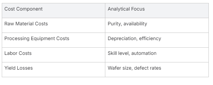
To maintain a grasp on economics, the industry employs various cost models and analytical formulas designed to predict and control wafer costs. Based on extensive data analysis, these models look at parameters like:
By using these models, manufacturers can estimate costs associated with different wafer sizes and process technologies, forecast pricing, and plan for future technological advances.
The silicon wafer industry’s ability to harness these analytical tools is key to navigating the complex web of cost factors and maintaining a competitive edge in the high stakes world of semiconductor manufacturing.
