

Physical design engineers are responsible for creating integrated circuits (ICs) and SoCs by designing layouts. One of the important considerations in IC design is power consumption. Here are some tips for physical design engineers to save power:
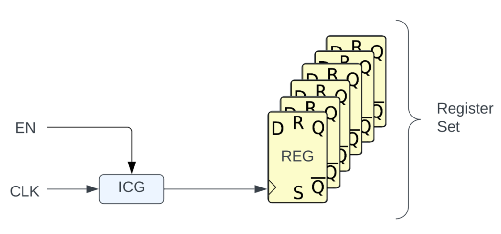
One of the most effective ways to reduce power consumption in electronic circuits is through clock gating. This technique involves turning off the clock signal when a particular logic block or module is not required for operation. By doing so, the unused portions of the circuit do not consume power unnecessarily. Clock gating is accomplished by using an integrated clock gating (ICG) cell, and it reduces the dynamic power (switching and internal) consumption of the design.
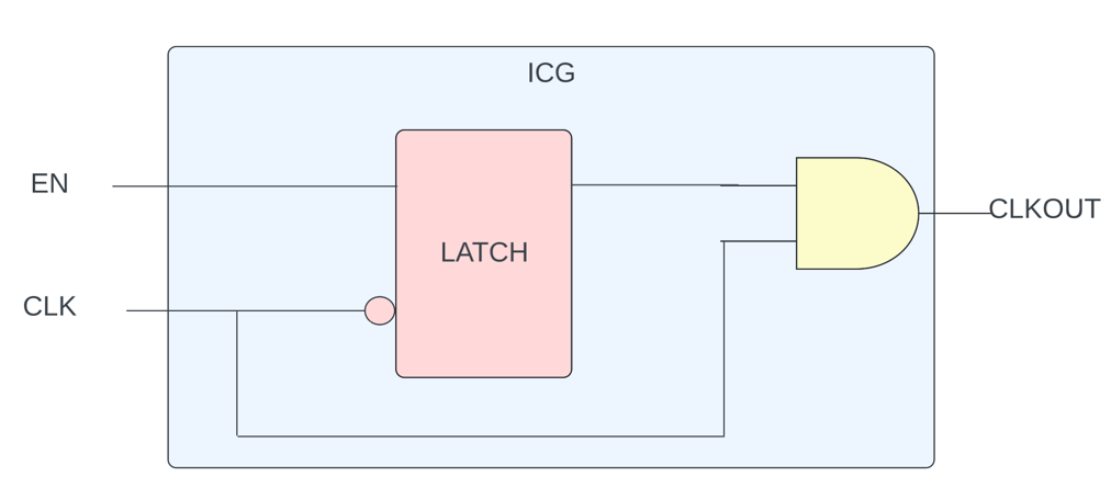
Clock gating can be fine-grained or coarse-grained, that allows the SOC designers to selectively gate different regions of the design for different use cases.
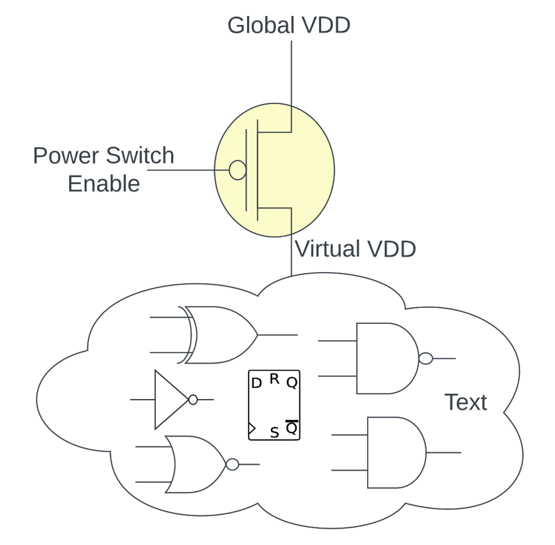
Power gating involves shutting down the entire circuit block when it’s not being used. When the module needs to start working again, it gets a supply for power and starts functioning normally. This technique requires an additional power switch (header or footer) to turn on and off the power supply to the standard cell logic. Normally, the standard cells lose their output states once they are power gated. In order to prevent the loss of state, designers may choose state retention registers which are special cells that can retain their state even when the voltage supply is turned off.
DFS technique adjusts the frequency of the clocks to reduce its power consumption. For instance, some applications do not require high-performance during runtime; an engineer optimizes it so that the CPU will go into a low-power idle mode since most of the frequency demand can wait.
Another application of DFS is where there are temperature sensors placed in the SoC design, particularly at locations which tend to have high switching activity, little to no clock gating etc. When the temperature sensor detects temperature higher than a certain threshold, it sends the signal to clock generator to reduce the clock frequency to bring the temperature back to normal at the cost of lower performance. This is essential because high temperatures caused due to high switching can have profound impact on the circuit reliability by slowing down the standard cells, electromigration issues and voltage drop issues.
Low-power library vendors optimize libraries to avoid leakage current issues associated with static CMOS or FINFET circuits. Libraries with multiple threshold voltage specifications and alternative topology choices further improve the power-performance trade-offs in layouts. Typically, any standard cell library offers following choices:
Physical design tools are good at making these trade-offs on a path by path basis and would tend to use more ULVT or LVT cells along a timing critical path and choose HVT cells on a path with positive setup slack to keep the overall leakage power of the design in check.
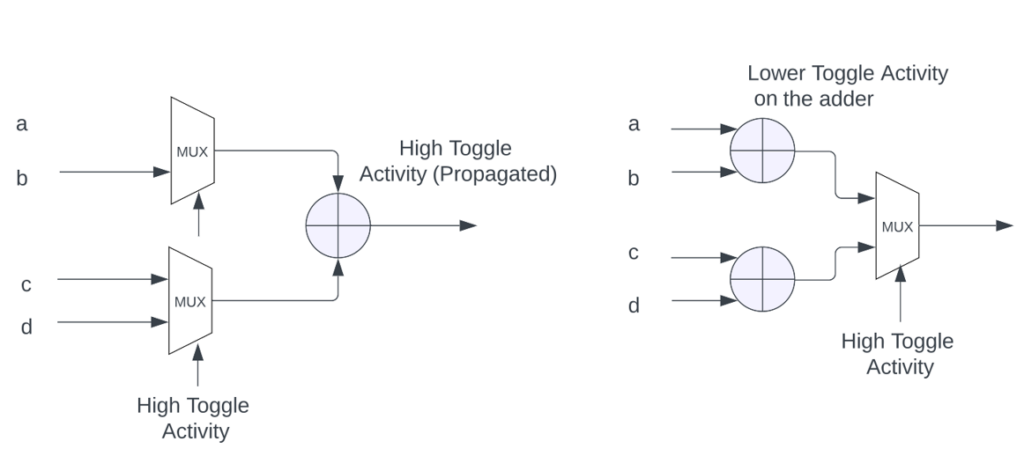
During an operation, unused stages of the pipeline can shut down and stop drawing power. Optimization of pipeline length has been shown to have dramatic effects on reducing dynamic power consumption. Also, smart RTL design can help push high toggle activity logic downstream to save dynamic power. As an example, in the figure below, by pulling the adders before the multiplexer designers can save power at the cost of some increased logic area.
By applying tools like “place and route” algorithms assists Physical designers in minimizing power consumption while also ensuring proper timing constraints concurrently.
Minimizing leakage current through changing CMOS technology node, leverage bump placement in SoC (system-on-a-chip), any logical optimizations or techniques like cell redundancy insertion might help one avoid undesired asymmetric leakage currents generated from process variations.
A dense routing structure may exhibit unwanted parasitic capacitance and resistance properties unless specific conductive materials are used. These factors result in higher leakage currents, leading to more power usage. As such, careful planning of metal layers and vias necessitates minimizing cross-connections helps designers deliver efficient power usage by reducing unnecessary penalties due to popular connection styles. In addition to minimizing the wire capacitance, routing optimizations also help with:
Place-and-route tools play an important role in generating layouts where switching activities and timing-critical signals are localized. A suitable placement of cells ensures these high-frequency nets stay short and isolated from noisy I/O pads, power supplies, or fast-moving parts within the design. Proper placement strategies can improve chip-area utilization without any drop-in functionality.
SAIF (Switching Activity Interchange Format) files can capture the toggle rates and the toggle counts of the signals in the design. Physical implementation tools can propagate the activity from the SAIF files and pull the logic with high toggle activity closer together to minimize the wire capacitance and therefore save dynamic power. SAIF based optimization is known to achieve up to 8% reduction in dynamic power.
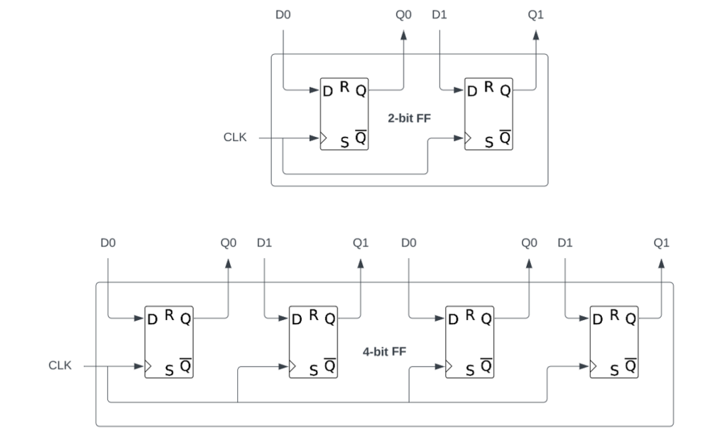
Multi-bit registers refer to design of a composite standard cell with two or more registers packaged as a single standard cell. It is quite common to have a 2-bit register, 4-bit register and an 8-bit registers as part of the standard cell library. Using multi-bit registers offer following advantages:
However, on the flip side, using multi-bit registers makes the last mile timing closure or any ECO (engineering change order) changes a bit challenging due to limited flexibility to push or pull the clock.
The operating voltage of the circuits play a key role in determining the performance of standard cells. However, not all the sub-blocks are critical to performance, and therefore designers can exploit this property to operate non-critical blocks are a lower voltage in contrast to the performance critical blocks like the CPU. In addition to operating at a lower voltage, these blocks can also work on a voltage that can be scaled up or down depending on the need to save power, as power is proportional to the square of the voltage. This is called Voltage Scaling and it helps adjusting the voltage levels of specific regions without sacrificing the overall system performance.
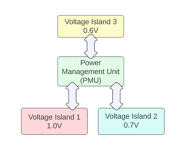
The cost of implementing multi-voltage islands is the need for level shifters to convert signals from one voltage domain to another, depending on the voltage domain crossing from either high to low voltage or low to high voltage. This ensures proper data transfer and synchronization.
In conclusion, physical design engineers use many methods to reduce power consumption. These techniques include clock gating, power gating, DVFS, optimization of routing, power-aware placement, and relocating the low-power libraries. A combination of these strategies may be used together to achieve better efficiency and lower energy consumption across electronic systems.
In summary, physical design engineers can apply various methods to minimize power usage in their designs, including Clock Gating, power Gating, and Dynamic Voltage Frequency Scaling. Selecting low-power libraries, pipeline optimization, layout optimizations and effective leakage avoidance methods are vital too. A holistic approach in assessing the benefits of these techniques can lead you to a well-balanced result with performance goals achieved while not sacrificing energy efficiency when implemented carefully.


