
Understanding the semiconductor manufacturing cost breakdown is essential before starting a custom chip, ASIC, or semiconductor production project.
The cost of manufacturing a semiconductor device is not only the wafer price. A complete cost model may include design, mask sets, wafer fabrication, wafer sort, packaging, final test, qualification, yield loss, logistics, engineering support, and long-term production management.
For a company developing a custom ASIC, the biggest question is often simple:
How much will it really cost to manufacture my chip?
The answer depends on the process node, die size, wafer diameter, yield, package type, test complexity, production volume, and whether the project uses MPW prototyping or a full mask set.
AnySilicon helps companies understand these cost drivers and connect with semiconductor partners for ASIC design, wafer fabrication, packaging, testing, and production supply.
A complete semiconductor manufacturing cost breakdown usually includes several major cost categories:
For ASIC projects, manufacturing cost is usually divided into two groups:
This distinction is important because an ASIC can have high upfront cost but attractive unit cost at volume.
Below is a simplified view of the main cost components.
| Cost Component | One-Time or Recurring? | What It Includes | Main Cost Drivers |
|---|---|---|---|
| Feasibility study | One-time | Initial cost, schedule, die size, process, and package estimate | Complexity, available specification, technology choice |
| IC design | One-time | Analog, digital, mixed-signal, RF, or high-voltage design | Design complexity, verification effort, IP content |
| IP licensing | One-time and/or recurring | Third-party IP blocks such as interfaces, processors, memory, analog IP | IP type, usage rights, volume royalties |
| EDA tools | One-time/project cost | Design, simulation, verification, layout, signoff tools | Tool flow, project duration, design team size |
| Mask set | One-time | Photomasks used for wafer fabrication | Process node, number of layers, wafer technology |
| MPW shuttle | One-time/prototype | Shared-mask prototype run | Die area, node, shuttle schedule, number of samples |
| Wafer fabrication | Recurring | Foundry processing of wafers | Node, wafer diameter, process options, volume |
| Wafer sort/probe | Recurring | Testing dies at wafer level | Test time, probe card, test coverage, temperature |
| Dicing | Recurring | Cutting the wafer into individual dies | Die size, wafer thickness, handling requirements |
| Packaging/assembly | Recurring | Assembling die into package | Package type, pin count, thermal needs, complexity |
| Final test | Recurring | Testing packaged ICs | Test time, equipment type, temperature, coverage |
| Qualification | One-time/project cost | Reliability and quality validation | Automotive, medical, industrial, aerospace requirements |
| Yield loss | Recurring impact | Cost of defective or rejected die | Die size, process maturity, design margin, defect density |
| Logistics and production management | Recurring | Shipping, inventory, planning, quality reporting | Volume, locations, supply chain complexity |
A semiconductor cost breakdown must separate NRE cost from unit cost.
NRE stands for non-recurring engineering. These are upfront costs needed to develop and prepare the chip for production.
NRE may include:
NRE is usually paid before volume production begins.
Unit cost is the recurring cost of manufacturing each chip.
Unit cost may include:
A custom ASIC becomes financially attractive when the unit-cost savings justify the NRE investment.
Share your project details and AnySilicon will help you identify the right semiconductor partners and cost drivers for your chip project.
The process node is one of the biggest cost drivers.
Advanced nodes usually require more expensive wafer processing, more complex masks, more design effort, and more verification. Mature nodes are often more cost-effective for analog, mixed-signal, industrial, automotive, sensor, and power-related ASICs.
For example, cost discussions around leading-edge nodes often reference very high wafer and mask costs, while mature-node ASIC projects can be much more practical for many industrial and mixed-signal applications. Recent industry cost guides estimate leading-edge 3nm wafer fabrication at around tens of thousands of dollars per wafer, while mask sets at the most advanced nodes can reach tens of millions of dollars. These figures vary widely by foundry, design, volume, and commercial agreement.
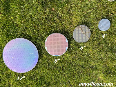
Semiconductor wafers are commonly manufactured on different wafer diameters, including 150mm, 200mm, and 300mm.
Larger wafers can produce more dies per wafer, but the equipment, process availability, and foundry ecosystem differ by node and technology.
Many analog, power, sensor, and specialty technologies are still manufactured on mature 150mm or 200mm lines, while many advanced digital processes use 300mm wafers.
Die size has a direct impact on cost.
A larger die means:
Reducing die size can significantly improve the economics of a semiconductor product, especially at high volume.
A simplified way to estimate chip cost is:
Cost per good die = wafer cost / number of good dies per wafer
Where:
Number of good dies = gross dies per wafer × yield
This formula is simplified but useful for early estimation.
Example:
Then you still need to add:
This is why the wafer cost alone does not represent the complete chip cost.
Yield is one of the most important factors in semiconductor manufacturing cost.
Yield refers to the percentage of chips that pass manufacturing and test requirements.
Yield is affected by:
Even a small yield change can significantly affect cost per good die, especially for large dies or advanced processes.
A mask set is required for full wafer fabrication. It contains the photomasks used to pattern the chip layers during manufacturing.
Mask set cost depends on:
Mask cost is a major reason why many companies use MPW shuttles for early prototypes. In an MPW shuttle, several designs share the mask and wafer run, reducing the cost for each participant. AnySilicon’s MPW cost guide explains that a typical MPW fee often includes access to a shared mask set, wafer fabrication for the die area, basic foundry processing, and a limited number of raw dies.
Wafer fabrication is the cost paid to process wafers through the foundry.
Wafer fabrication cost depends on:
For many ASICs, wafer fabrication is the largest recurring manufacturing cost before packaging and test.
Packaging protects the die and provides electrical connection to the system board.
Packaging cost depends on:
Common package options include:
A simple package may be inexpensive, while advanced packaging can become a major part of the total chip cost, especially for high-performance processors, AI accelerators, RF devices, and multi-die systems.
Testing is often underestimated.
Semiconductor test cost depends on:
A simple digital device may be faster to test than a precision analog, RF, sensor, high-voltage, or automotive-grade IC.
Test cost can become significant when:
Qualification cost depends heavily on the target market.
Consumer products may require a lighter qualification flow than automotive, medical, aerospace, industrial safety, or defense applications.
Qualification may include:
Qualification is often a one-time project cost, but it can affect schedule and production readiness.
Production volume affects both NRE recovery and unit cost.
At low volume, NRE dominates the economics. At high volume, unit cost becomes more important.
This is why custom ASICs usually make more sense when there is enough production volume to justify the upfront development cost.
A company considering an ASIC should ask:
Below is a simplified example for illustration.
| Item | Example Value |
|---|---|
| Wafer cost | $4,000 |
| Gross dies per wafer | 1,200 |
| Yield | 80% |
| Good dies per wafer | 960 |
| Wafer cost per good die | $4.17 |
| Wafer sort | $0.30 |
| Dicing | $0.05 |
| Packaging | $0.60 |
| Final test | $0.40 |
| Logistics and production support | $0.20 |
| Estimated manufacturing cost per unit | $5.72 |
This is only a simplified model. Real projects may have much higher or lower costs depending on node, die size, package, test time, volume, yield, and commercial terms.
Cost drivers:
These projects may have relatively manageable manufacturing costs, but analog design, layout, and test quality are critical.
Cost drivers:
Mixed-signal ASICs often require careful planning because both design and test can become complex.
Cost drivers:
Advanced digital chips can require high NRE and high mask costs, especially at leading-edge nodes.
Cost drivers:
RF test and characterization can be a major part of the total cost.
Cost drivers:
These projects often use mature specialty processes rather than leading-edge digital nodes.
One of the most important cost decisions is whether to use an MPW shuttle or a full mask set.
MPW is usually used for early prototypes.
Benefits:
Limitations:
A full mask set is usually needed for production.
Benefits:
Limitations:
For many custom ASIC projects, the best path is to prototype through MPW first and move to a full mask set once the design is validated.
Companies can reduce semiconductor manufacturing cost by making good decisions early.
Possible cost-reduction methods include:
Do not automatically choose the most advanced node. Many products can be built more economically on mature nodes.
Smaller die size usually improves cost per good die and yield.
Each IP block may add licensing cost, verification effort, die area, and integration risk.
Design-for-test can reduce production test time and improve quality.
The cheapest package is not always the best, but over-specifying the package can increase cost unnecessarily.
Yield improvement can have a large effect on cost per unit.
MPW can reduce early prototype cost before committing to full-mask production.
Some suppliers are better suited for low-volume specialty products. Others are optimized for high-volume production.
Wafer cost is important, but it is not the full cost. Packaging, test, yield, qualification, logistics, and production support also matter.
A low wafer price does not help if the yield is poor.
Test cost can be significant, especially for analog, RF, high-voltage, and automotive devices.
Advanced nodes may increase mask, wafer, design, and verification cost without improving the business case.
ASIC economics must include upfront NRE, not only recurring unit cost.
A custom chip may be used for many years. Long-term supply and lifecycle planning should be included in the cost model.
Estimating semiconductor manufacturing cost requires more than a simple wafer price.
You need to understand:
AnySilicon helps companies connect with semiconductor partners for ASIC design, wafer fabrication, packaging, testing, qualification, and production supply.
Semiconductor manufacturing cost may include wafer fabrication, mask sets, wafer sort, dicing, packaging, final test, qualification, yield loss, logistics, and production support.
The biggest cost depends on the project. For many ASICs, wafer fabrication and yield are major recurring cost drivers. For advanced-node chips, mask sets and design NRE can also be very large. For high-performance chips, advanced packaging and memory can be significant cost drivers.
NRE means non-recurring engineering. It includes upfront costs such as design, verification, layout, IP licensing, mask sets, prototype fabrication, test development, and qualification.
A simplified calculation is: wafer cost divided by the number of good dies per wafer, plus packaging, test, logistics, and production support. The number of good dies depends on die size and yield.
Larger dies reduce the number of chips per wafer and are more sensitive to defects. This usually increases the cost per good die.
Yield determines how many chips pass manufacturing and test. Lower yield increases the cost of each good chip because the cost of failed chips must be absorbed by the good units.
MPW allows several designs to share mask and wafer costs, making it useful for prototypes. Full mask production gives more control and is usually needed for volume manufacturing, but it has higher upfront cost.
Yes. AnySilicon helps companies connect with ASIC design, foundry, packaging, testing, and turnkey manufacturing partners that can support cost estimation and production planning.


