

Wafer inspection is a critical step in semiconductor manufacturing, ensuring the quality and reliability of integrated circuits. It involves a series of rigorous tests and examinations performed at various stages of the fabrication process to detect defects, contamination, and deviations from specified parameters. These inspections utilize a range of techniques, including optical microscopy, scanning electron microscopy (SEM), and automated optical inspection (AOI) systems, to identify issues such as scratches, particles, and structural imperfections. The data gathered during inspection helps to optimize manufacturing processes, improve yield, and prevent defective wafers from progressing further in the production line, saving time and resources.

Wafer inspection is vital in semiconductor manufacturing, ensuring the quality and reliability of electronic devices. This process identifies defects on wafers, which are thin slices of semiconductor material.
Key Wafer Inspection Tools
Types of Defects
Wafer inspection systems play a crucial role in both incoming and outgoing quality control during high-volume manufacturing. These systems help detect a wide range of defects, enhancing yield and reducing costs.
Monitoring Technologies
With these methods, device manufacturers can achieve high quality in the semiconductor manufacturing process, ensuring the reliability of electronic devices.
Wafer inspection technologies are essential in the semiconductor industry to ensure the quality and efficiency of electronic devices. These systems detect defects at various points in the manufacturing process, enhancing overall yield and reducing production costs. By utilizing advanced inspection methods, manufacturers can accurately identify defects, whether they are random or systematic. This improves the quality control during both incoming and outgoing inspections, ensuring that high standards are maintained throughout the production cycle. Inspection systems are continually evolving to keep pace with the demands of high-volume manufacturing, making them crucial for companies aiming to remain competitive in the electronic device market.
Confovis and INSPECTRA® Series: Advanced Defect Detection
The Confovis and INSPECTRA® Series systems provide cutting-edge solutions in defect detection for the semiconductor industry. These advanced tools employ sophisticated inspection technologies to identify a wide range of defects on semiconductor wafers. By focusing on precision and accuracy, the Confovis systems help pinpoint even the most minor imperfections that could impact the reliability of the final product. The INSPECTRA® Series is known for its high throughput and ability to maintain consistency in inspections, which is vital in high-volume manufacturing environments. Both systems ensure that device manufacturers can confidently produce high-quality electronic devices.
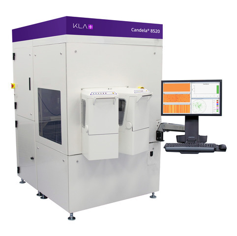
KLA-Tencor’s Surface Inspection Systems
KLA-Tencor’s surface inspection systems are leaders in the field, known for their ability to deliver detailed analyses of wafer surfaces. These systems use a combination of brightfield and darkfield inspection techniques to identify various types of defects, from small random defects to larger systematic ones. As a result, manufacturers can catch defects early in the process, allowing for corrective measures that enhance the overall yield. KLA-Tencor’s systems also excel in providing comprehensive data that can be used for continuous improvement in wafer processing. This ensures that every semiconductor wafer meets the highest quality standards before moving to the next stage of production.
Takano’s Micro-Bump Inspection Tools
Takano’s micro-bump inspection tools are essential for examining the tiny features present on modern semiconductor devices. These tools specialize in assessing the micro-bumps that are crucial for connecting different layers within electronic devices. By detecting defects at this microscopic level, Takano’s tools ensure that the internal connections within a device are reliable and robust. The accuracy and sensitivity of these tools help prevent issues such as short circuits or disconnects, which could lead to device failure. For manufacturers, using Takano’s micro-bump inspection tools means maintaining the integrity and performance of next-generation electronic devices, catering to the increasing demands for miniaturization and higher functionality.
Integration of Artificial Intelligence in Wafer Inspection
The integration of Artificial Intelligence (AI) in wafer inspection is transforming the semiconductor manufacturing process. AI technologies enhance the defect detection capabilities of wafer inspection systems. This leads to higher quality standards in electronic devices. The AI-driven inspection process analyzes data at a quicker pace and with higher accuracy than traditional methods. By using AI, manufacturers can improve inspection throughput, making high-volume manufacturing more efficient. Wafer inspection tools powered by AI can adapt to different defect inspection applications, providing a wide range of solutions to detect both random and systematic defects.


