

Ball Grid Array, commonly known as BGA, is one of the most widely used semiconductor package types for integrated circuits that require a high number of I/O connections, good electrical performance, reliable board mounting and efficient use of PCB area.
In a BGA package, the external connections are arranged as an array of solder balls on the bottom side of the package. This allows the package to support more connections than traditional leaded packages where pins are placed only around the perimeter. BGA packages are commonly used for processors, ASICs, FPGAs, memory devices, wireless chips, networking devices, automotive ICs and many high-performance electronic systems.
Compared with older package styles such as PGA, QFP or leaded packages, BGA technology enables higher pin density, shorter electrical paths, improved board-level reliability and better use of package area. However, BGA packages also require more advanced assembly, inspection and PCB design practices.
AnySilicon can help semiconductor companies connect with IC packaging and assembly vendors for BGA, FBGA, FCBGA, WFBGA, CABGA, PBGA, lidless BGA and custom substrate-based packages.
Typical vendor support may include package selection, substrate design, wire-bond BGA, flip-chip BGA, ball map review, assembly, package qualification, production ramp and final test coordination.
With the levels of integration rising to unprecedented levels and the requirement of integrated circuits with a high number gate and pins increased day by day, there was a need to manufacture a package that would be convenient to use, would be will reliable and robust, would pose higher pin count, improved performance while simultaneously reducing package size and thickness — that is when BGA technology came into the picture.

Figure 1 – BGA Package: top, bottom and side views (courtesy: Amkor Technology)
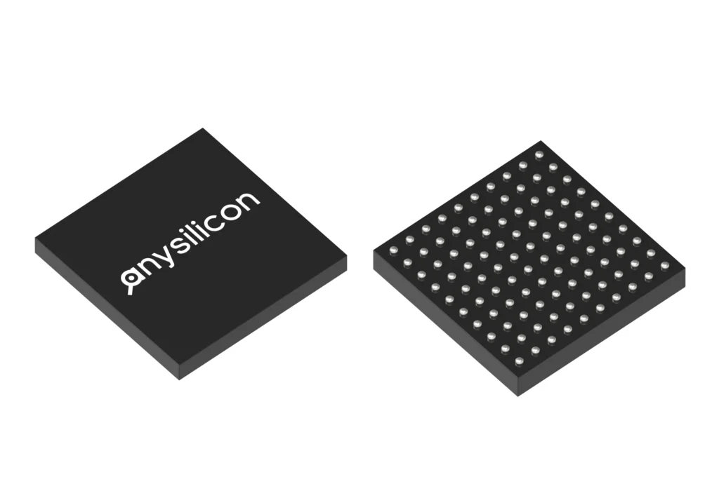
BGA , or Ball Grid Array, is a kind of a surface mount package which is used in electronic products to mount integrated circuits such as microprocessors, FPGAs, WiFi chips etc. The pins are in the form of solder balls that are arranged in a grid like pattern on the undersurface of the package to increase the area used for the connections rather than just the periphery.
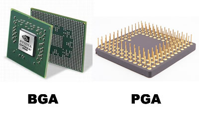
Figure 2: BGA package vs PGA package
BGA has evolved from the PGA package. In a PGA or Pin Grid Array, you would see an array of pins arranged in a grid of one, two or more rows and are used to connect the chip to the printed circuit board so that electrical signals may be conducted between them through the pins. In a BGA, however, these pins are replaced with a number of solder balls (surface mount technology or SMT) attached to the undersurface of the package with the help of pads and flux through a very precise automated process.
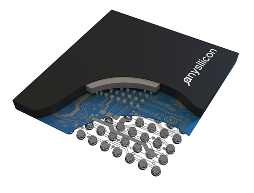
There are 2 types of methods used today to connect the silicon die to the substrate: Wirebond and FlipChip. A wireboned BGA package uses wires to connect the silicon die to the substrate. A flipchiped package utilizes bumps as shown in the following figure.
BGA packages usually include:

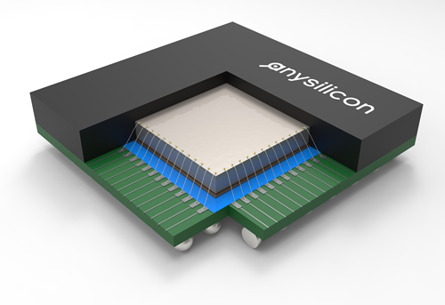
Figure 3: Flip Chip BGA internal construction
The substrate is a small PCB with traces designed specifically for your package. The substrate is used for connecting the bumps to the solder balls and consists of several layers to meet the design complexity. The substrate material needs is selected to meet the signal integrity requirements, for example for RF signals a special material should be used to ensure the substrate does not reduce the signal quality.
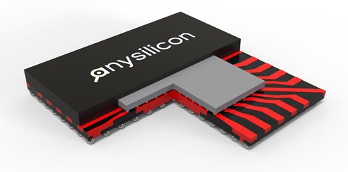
In a wire-bond BGA package, the die is attached to the substrate and thin metal wires connect the die pads to bond fingers on the substrate. The substrate then routes those signals to the BGA solder balls.
In a flip-chip BGA package, the die is flipped and connected directly to the substrate using solder bumps, copper pillars or similar interconnect structures. This approach provides shorter electrical paths and can support higher I/O density and higher performance.
Get an indicative packaging cost range, then a detailed breakdown by email.
There are a multitude reasons why Ball Grid Array packages are increasingly being preferred in various applications, some of which are detailed below:
Higher pin density
In order to improve performance/features/price, we saw that manufacturers would increase the number of pins on a package but compromise on the quality as the pins would be placed too close together and the soldering joints would come out to be weak and unreliable in the process. With BGA packages, we obtain hundreds of pins on a single package without compromising on the quality of the soldering or the reliability of the package.
Lower inductance
Since the connecting conductors are short in length as compared to longer wires, it lowers the inductance of the signals which improves their electrical performance as lowering inductance.
Better heat conduction
Again, the decreased distance and inductance between the BGA package and the circuit board makes for lower thermal resistance between the two components which allows smoother and better flow and conduction of heat through the board. In addition to that – a very good lid to dissipate the heat directly from the die. This significantly reduces chip overheating and thermal damage events.
Increased performance
All of these factors ultimately result in a much better electrical performance by the Ball Grid Array as compared to other IC packaging technologies. Utilizing bumping technology with a suitable substrate material gives it superior performance at high speed.
Difficult inspection
While the soldering helps improve the performance of the package and the circuit as a whole, it does not come without its disadvantages, with the main issue being the inability to inspect the package once it has been soldered onto the circuit board. As such, it can be difficult to identify any potential faults and fix them since you cannot view the surface like you would be able to with a PGA package. To counter this package density, the likes of X-rays and CT scanning are used to inspect for any aberrations in the circuit or the connections, although the process may prove to be expensive.
Somewhat expensive
While there may be some IC package solutions out there that may cost you less, using BGA packages are relatively expensive. The bumping process and the substrate are cost adders compared to, for instance, a QFN package.
Choosing between wire-bond BGA and flip-chip BGA depends on cost, performance, I/O count, package size, power dissipation and product requirements.
| Feature | Wire-Bond BGA | Flip-Chip BGA |
|---|---|---|
| Die connection | Wire bonds from die pads to substrate | Bumps or copper pillars connect die directly to substrate |
| Cost | Usually lower | Usually higher |
| I/O density | Moderate | High |
| Electrical performance | Good for many applications | Better for high-speed and high-performance devices |
| Thermal performance | Depends on package design | Often better, especially with lid or heat spreader |
| Typical use | Analog, mixed-signal, MCU, ASICs, moderate I/O devices | Processors, AI chips, networking ICs, high-speed SoCs, advanced ASICs |
Wire-bond BGA can be a cost-effective option for many ASIC and mixed-signal designs. Flip-chip BGA is often selected when the design requires higher performance, higher I/O density, better power distribution or shorter interconnect paths.
The substrate is one of the most important parts of a BGA package. It acts like a small, high-density PCB inside the package and routes signals between the silicon die and the solder balls.
A BGA substrate may include multiple metal layers, vias, power and ground planes, routing channels and controlled impedance traces. The substrate design affects package cost, manufacturability, signal integrity, power integrity, thermal performance and reliability.
Key substrate design considerations include:
For high-speed, RF, AI, networking or advanced ASIC applications, substrate design can become a major part of the packaging development process.
BGA is not one single package. It is a family of package types with different materials, sizes, thermal structures, pitches and assembly methods. The right BGA type depends on the application, I/O count, performance requirements, cost target and reliability needs.
PBGA is one of the most common BGA package types. It uses a plastic molded package body and an organic substrate. PBGA is widely used for many commercial and industrial ICs because it offers good performance at a reasonable cost.
Typical applications include ASICs, microcontrollers, communication devices, consumer electronics and mixed-signal ICs.
FBGA uses a finer solder ball pitch than standard BGA packages. It is useful when the device requires a smaller package footprint while still maintaining a relatively high number of I/O connections.
FBGA is commonly used in memory devices, mobile electronics, wireless chips and compact systems where board space is limited.
FCBGA uses flip-chip interconnect technology to connect the die directly to the substrate. This package type supports high I/O density, improved electrical performance and better power delivery compared with many wire-bond BGA options.
FCBGA is often used for processors, GPUs, networking devices, AI accelerators, high-performance ASICs and advanced SoCs.
WFBGA is a thin fine-pitch BGA package used where low package height and small footprint are important. It is common in compact electronic products such as mobile devices, wearable electronics and portable systems.
CABGA is a compact BGA package type often used when a near-die-size package is needed. It can be attractive for applications where cost, size and I/O density need to be balanced.
HSBGA includes a heat spreader to improve thermal performance. It is used when the IC dissipates more power and requires better heat transfer from the die to the surrounding environment.
FCHSBGA combines flip-chip interconnect with a heat spreader. This package type is used for higher-performance devices where both electrical performance and thermal management are important.
TEPBGA is designed to improve thermal performance compared with standard plastic BGA packages. It may include thermal enhancements that help transfer heat away from the die.
CBGA uses a ceramic substrate or ceramic package construction. It is often selected for high-reliability, high-temperature, aerospace, defense, RF or harsh-environment applications.
OBGA uses an organic substrate material. Many modern BGA packages use organic laminate substrates because they can support high routing density and cost-effective manufacturing.
TBGA uses a tape-based substrate structure. It can be used in applications where thin package construction, flexibility or specific electrical characteristics are needed.
TFBGA is a thin fine-pitch BGA package. It is used when the design needs a low-profile package with relatively dense I/O connections.
LBGA is a lower-height BGA package. It is used where package thickness is important, such as compact modules, portable electronics and space-constrained boards.
LFBGA combines low package height with fine-pitch solder balls. It is commonly used in compact electronic systems that require both small size and higher I/O density.
Micro BGA, or μBGA, is a small BGA package with very fine ball pitch. It is used in compact and high-density applications where the package must be as small as possible.
| BGA type | Main advantage | Typical use |
|---|---|---|
| PBGA | Cost-effective and widely available | General ASICs, MCUs, mixed-signal ICs |
| FBGA | Smaller footprint and fine pitch | Memory, mobile, compact electronics |
| FCBGA | High performance and high I/O density | Processors, AI, networking, advanced SoCs |
| WFBGA | Thin and compact | Mobile, wearables, portable electronics |
| CABGA | Near-die-size and compact | Cost-sensitive compact ICs |
| HSBGA | Better thermal performance | Higher-power ICs |
| FCHSBGA | Flip-chip performance plus thermal support | High-performance ICs |
| TEPBGA | Thermally enhanced plastic package | Power-sensitive ICs |
| CBGA | High reliability and temperature capability | Aerospace, defense, RF, harsh environments |
| OBGA | Organic substrate-based BGA | Broad commercial and advanced applications |
| TBGA | Tape-based package structure | Thin or specialized applications |
| TFBGA | Thin fine-pitch package | Space-constrained electronics |
| LBGA | Low package height | Compact electronic products |
| LFBGA | Low profile and fine pitch | Compact high-density systems |
| μBGA | Very small package size | Miniaturized electronics |
Choosing the right BGA package requires both technical and commercial review. The best option depends on the chip, application, volume and reliability requirements.
Important questions include:
The package decision should be made early in the ASIC or IC development flow because die pad placement, bump map, package substrate, PCB routing and test strategy are connected.
BGA package cost depends on the package type, substrate, assembly method, volume and reliability requirements.
Main cost drivers include:
A simple PBGA or wire-bond BGA is usually less expensive than a high-density flip-chip BGA with advanced substrate technology. However, the lowest-cost package is not always the best choice if it creates PCB routing, thermal, signal integrity or reliability problems.
Use the link below to get an indicative BGA packaging and assembly cost range. For an official quote, submit your email and project details, including package type, ball count, body size, annual volume, reliability level and target assembly region.
BGA stands for Ball Grid Array. It is a surface-mount IC package that uses an array of solder balls on the bottom side of the package for electrical connection to the PCB.
BGA packages are used for ICs that require higher I/O density, better electrical performance or more compact board mounting. Common examples include ASICs, processors, FPGAs, memory, wireless chips and networking devices.
BGA uses solder balls arranged across the bottom of the package, while QFN uses perimeter pads and often an exposed thermal pad. BGA is better for higher I/O count devices, while QFN is usually lower cost and used for lower-to-medium pin-count devices.
Wire-bond BGA connects the die to the substrate using bond wires. Flip-chip BGA connects the die directly to the substrate using bumps or copper pillars. Flip-chip BGA usually supports higher I/O density and better electrical performance, but it is typically more expensive.
FCBGA stands for Flip-Chip Ball Grid Array. It is a BGA package where the die is connected directly to the substrate using flip-chip interconnect technology.
FBGA stands for Fine Pitch Ball Grid Array. It is a BGA package with finer solder ball pitch, often used when a smaller package footprint is required.
PBGA stands for Plastic Ball Grid Array. It is a common BGA package type that uses a plastic molded body and organic substrate.
μBGA, or micro BGA, is a very small BGA package with fine ball pitch. It is used in miniaturized electronic systems where package size is very important.
BGA solder joints are located underneath the package, so they cannot be inspected directly by visual inspection. X-ray inspection is commonly used to check solder joint quality.
BGA packaging cost depends on package type, ball count, substrate layer count, body size, wire-bond or flip-chip assembly, volume, reliability level and assembly region. A simple wire-bond BGA is usually less expensive than an advanced flip-chip BGA.
AnySilicon can help connect semiconductor companies with IC packaging vendors based on package type, technical requirements, volume, location and production needs.
Looking for BGA packaging support? AnySilicon can help you find vendors for BGA package design, substrate design, wire-bond BGA, flip-chip BGA, FBGA, FCBGA, PBGA, CABGA, lidless BGA, package assembly and production ramp.
There is no doubt that BGA package type will be used for a long time. However, a few technology advancements have made it possible to develop more advanced types of BGA package which are cheaper and provide better electrical performance. The main two types are:
WLCSP – Wafer Level Chip Scale Package is essentially a bumped die. Read more about WLCSP here.
eWLB – embedded Wafer Level BGA is a bumped die with an interposer. Read more about eWLB here.
