

Since the development of the first ASIC, the IC package was a mean to protect the silicon die and to provide means to PCB connectivity. Back then, the IC package was large and introduced various electrical parasitic.
WLCSP package is one of the latest and most impressive invention of the semiconductor packaging industry. Today, with WLCSP, the package has the smallest possible package footprint and superior electrical and thermal performance.
The beauty in WLCSP package is the connectivity. The connectivity between the silicon die is merely bumps which offer low resistance, and low inductance. WLCSP is not cheap for low-mid volume production, but for many market segments and applications, WLCSP is the best choice in terms of price and performance.
WLCSP technology proves to be a reliable and robust and today used by millions every day in mobile phones, that are exposed to extreme variation in stress, drop and vibration.
Since WLCSP is a wafer level package, there are already several wafer foundries that offer WLCSP assembly services in house (TSMC, GLOBALFOUNDRIES and more), making the semiconductor manufacturing easier and cheaper for customers.
The Demand for WLCSP
In the last 2-3 decades, wireless, analog, mixed-signal and memory ICs have made a tremendous development in terms of functionality, gate density and performance — thanks to advancement in the semiconductor process technology. So much progress, that traditional package type such as QFN and BGA have become a barrier in reaching better and higher performance.
Typical QFN that is based on wirebond technology has high inductance and high wire resistance. While typical BGA utilizes a substrate to connect the die to the balls, introduce further wiring that reduce the overall IC preference.
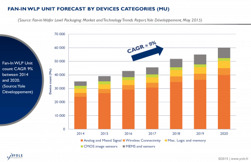
While the consumer market (especially mobile devices) where on the outlook to shrink the mobile device size or alternately pack more features into a hand-held products.
Fan In versus Fan Out Wafer Level Packaging
For semiconductor professional Fan-In WLCSP is a true wafer level packaging, because the pads (or bumps) are all within (under) the die footprint. While Fan-out WLCSP offers a package size beyond the size of silicon dies to allow higher bump pitch.
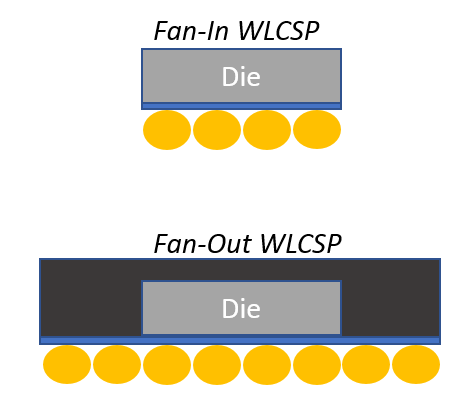
In both cases, no substrate is used to connect silicon die to the PCB. Balls (bumps) are directly attached to the silicon die or the fan-out area.
Fan-in WLCSP fits best to applications that utilize small dies and relatively low IO count. Fan-out WLCSP has the ability for larger footprint and therefore offers higher IO count.
Redistribution Layout (RDL)
RDL is an additional layer applied directly on wafers and act as a layout layer to help redistribute the fine pitch pads to a larger area.
Embedded Wafer Level BGA (eWLB)
To explain how eWLB wafer is created: first, the wafer is diced, and the dies are embedded in a new and larger molded wafer. Then the dies are disconnected from each other exactly by a distance which is the calculated fan-out area to be manufactured.
WLCSP is a type of semiconductor packaging technology that produces the smallest package size possible. In WLCSP, the package size is equivalent to the die size, unlike traditional packaging that utilizes a larger substrate. This is achieved by forming interconnections and bumps directly on the wafer before dicing, eliminating the need for a separate substrate.
Traditional packaging uses substrates like leadframes or laminates to mount and connect the die. In contrast, WLCSP eliminates the substrate and mounts the die directly onto the motherboard. This miniaturization is achieved by performing all the interconnection and bumping processes at the wafer level, leading to significant space savings.
WLCSP consists of three main components:
An RDL is a layer of copper interconnects used to reroute the input/output connections from the die bond pads to the bumps. This allows for a higher density of interconnects and greater design flexibility. RDLs are particularly beneficial in WLCSP due to the small size of the die and the need for efficient space utilization.
Wafer thinning involves grinding down the backside of the wafer to reduce its thickness. This process is crucial in WLCSP for minimizing the overall package height and enabling the stacking of multiple chips. By thinning the wafers, manufacturers can achieve significant space savings and create more compact devices.
WLCSP offers several advantages compared to traditional packaging methods:
There are two primary WLCSP structures:
WLCSP is widely used in various applications, including:
Get an indicative packaging cost range, then a detailed breakdown by email.


