


The health of the semiconductor industry is increasingly tied to the health of the worldwide economy. Rarely can there be strong semiconductor market growth without at least “good” worldwide economic growth to support it. Consequently, IC Insights expects annual global semiconductor market growth rates to continue to closely track the performance
Read More
SiFive, the first fabless semiconductor company to build customized, open-source enabled semiconductors, today announced its flagship Freedom family of system on a chip (SoC) platforms. Built around the free and open RISC-V instruction set architecture invented by the company’s founders at the University of California, Berkeley, SiFive’s Freedom U500 and
Read More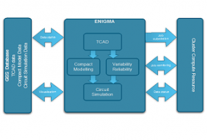
Synopsys, Inc. announced it has completed the acquisition of Gold Standard Simulations Ltd. (GSS), a leading provider of TCAD and EDA simulation solutions for design technology co-optimization (DTCO) of advanced process nodes. The acquisition of GSS supports the Synopsys TCAD strategy to offer a comprehensive solution to reduce development time and cost
Read More
All the work that’s been done on stacked die really could pay off soon.
The challenges of Moore’s law scaling at advanced technology nodes are well documented. I won’t repeat them here. The benefits of “more than Moore” scaling (i.e., 2.5D and 3D ICs) are also well-known. This technology

he Internet of Things is a fast-growing industry built on the promise of ubiquitous connectivity that will enable billions of devices to talk to each other and to people. The estimates for the number of IoT devices to ship by 2020 can vary widely, from the more conservative six billion figure presented
Read More
Semiconductor Manufacturing International Corporation (“SMIC”; NYSE: SMI; SEHK: 981), one of the leading semiconductor foundries in the world and the largest and most advanced foundry in mainland China, jointly announces with LFoundry Europe GmbH (“LFE”) and Marsica Innovation S.p.A. (“MI”), the signing of an agreement on June 24, 2016 to
Read More