

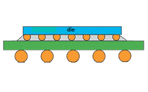
Yole Développement announces its Flip Chip Market and Technology Trends report. Yole Développement’s analysis updates the business status of the Flip-Chip market including data for TIM, underfills, substrates and Flip-Chip bonders. Discover fully updated 2010 – 2018 market forecast, detailed technology roadmap and bottom up approach, plus a strong focus
Read More
In the field of IC Design, there are many companies that have unique focus and experience in designing integrated circuits, as well as being involved in the other aspects of IC design house elements, such as packaging, testing, validation, et cetera.
It may seem like a simple choice to
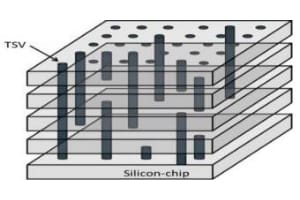
3D Through Silicon Vias (TSV) is in MEMS, CMOS Image Sensors and high-end applications. When will it be used for mainstream consumer applications?… All results are part of the new report released by Yole Développement (Yole): 3DIC & 2.5D TSV Interconnect for Advanced Packaging – 2014 Business Update. This technology
Read More
This is a guest post by Vidatronic which is a fabless semiconductor and systems company specializing in the design of advanced-architecture, energy-efficient power management solutions.
In the last few decades, technology has been growing at a spectacular rate. So, it only makes sense that the parts that make up our technology
Read More
This is a guest post by Methodics that delivers state-of-the-art semiconductor data management (DM) for analog, digital and SoC design teams.
No doubt that by now you have noticed that IP Lifecycle Management is a key Focus for Methodics and is a cornerstone of our platform for IP creators and SoC Integrators. Also
Read More
This is a guest post by PLDA which designs and sells intellectual property (IP) cores and prototyping tools for ASIC and FPGA
You are on a tight schedule for your next chip. Not wanting to reinvent the wheel, you plan to go to an outside vendor for some of your silicon
Read More