


body{font-family:Arial,Helvetica,sans-serif;color:#222;line-height:1.72;margin:0;background:#fff}
article{max-width:980px;margin:0 auto;padding:18px 18px 48px}
h1{font-size:38px;line-height:1.18;margin:0 0 20px}
h2{font-size:28px;line-height:1.3;margin:36px 0 14px}
h3{font-size:21px;line-height:1.35;margin:24px 0 10px}
p{margin:0 0 17px}
ul{margin:0 0 20px 22px;padding:0}
li{margin:0 0 7px}
table{width:100%;border-collapse:collapse;margin:18px 0 26px;font-size:15px}
th,td{border:1px solid #d9dde2;padding:11px 12px;text-align:left;vertical-align:top}
th{background:#f3f5f7}
.cta{background:#f6f7f8;border-left:5px solid #d71920;padding:22px;margin:28px 0}
.cta a{display:inline-block;background:#d71920;color:#fff;text-decoration:none;font-weight:700;padding:11px 18px;border-radius:3px}
.note{background:#fff8e8;border:1px solid #eedda7;padding:15px 17px;margin:20px 0}
.small{font-size:13px;color:#666}
@media(max-width:700px){h1{font-size:31px}h2{font-size:24px}table{font-size:14px}}
body{font-family:Arial,Helvetica,sans-serif;color:#222;line-height:1.72;margin:0;background:#fff}
article{max-width:980px;margin:0 auto;padding:18px 18px 48px}
h1{font-size:38px;line-height:1.18;margin:0 0 20px}
h2{font-size:28px;line-height:1.3;margin:36px 0 14px}
h3{font-size:21px;line-height:1.35;margin:24px 0 10px}
p{margin:0 0 17px}
ul{margin:0 0 20px 22px;padding:0}
li{margin:0 0 7px}
table{width:100%;border-collapse:collapse;margin:18px 0 26px;font-size:15px}
th,td{border:1px solid #d9dde2;padding:11px 12px;text-align:left;vertical-align:top}
th{background:#f3f5f7}
.cta{background:#f6f7f8;border-left:5px solid #d71920;padding:22px;margin:28px 0}
.cta a{display:inline-block;background:#d71920;color:#fff;text-decoration:none;font-weight:700;padding:11px 18px;border-radius:3px}
.note{background:#fff8e8;border:1px solid #eedda7;padding:15px 17px;margin:20px 0}
.small{font-size:13px;color:#666}
@media(max-width:700px){h1{font-size:31px}h2{font-size:24px}table{font-size:14px}}

Sony Semiconductor Solutions and Taiwan Semiconductor Manufacturing Company have signed a non-binding memorandum of understanding to explore a strategic partnership for the development and manufacturing of next-generation CMOS image sensors. Under the proposed structure, the two companies intend to establish a joint venture in Japan, with Sony expected to be
Read More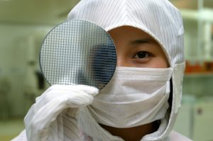
The ams OSRAM 2026 MPW (Multi-Project Wafer) program expands its technology offering with new 180nm options, including the C18 CMOS specialty platform further enriching the MPW portfolio. For mixed-signal designs in mature nodes, this extension delivers strong analog, high-voltage and BCD capabilities tailored to customer needs.
The MPW program

Choosing between 28nm, 40nm, and 65nm is one of the most common — and most underestimated — decisions in ASIC development.
These nodes dominate industrial, automotive, consumer, and IoT ASICs, yet teams often choose based on habit or outdated assumptions. In reality, the differences between 28nm, 40nm, and 65nm
Choosing a 22nm process node is not just a scaling decision — it is a strategic choice that affects power consumption, cost structure, ecosystem access, and long-term product risk.
For many ASIC and SoC teams, 22nm sits at the crossroads between mature nodes (28nm/40nm) and more advanced, higher-risk technologies.