

Multi-Project Wafer (MPW) runs are often described as a low-cost way to get first silicon. That’s true — but only if you understand what the MPW fee actually includes and, just as importantly, what it does not.
Many first-time teams underestimate MPW cost, not because MPW is expensive, but

This interview with Jens Milnikel, EVP & GM, CMOS Sensors ASICs (CSA) at ams OSRAM, reveals not just the technologies and strategies driving the CSA business of ams OSRAM, but the human stories, partnerships, and vision that set it apart as a true leader in the future of sensing solutions.
Read More
To understand SkyWater’s origins, one must first rewind to the convergence of national security and semiconductor manufacturing. For decades, the U.S. military and intelligence agencies relied on advanced microelectronics built on American soil. Semiconductors powered guidance systems, radars and signal processors from the Cold War era onward.
At the
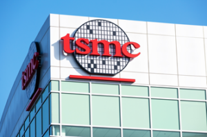
October 21, 2025 — Hsinchu, Taiwan — Taiwan Semiconductor Manufacturing Company (TSMC), the world’s leading semiconductor foundry, today announced plans to break ground on its new 1.4 nanometer (A14) fabrication facility in Taichung, Taiwan, on November 5, 2025. The groundbreaking marks a major milestone in TSMC’s ongoing roadmap toward next-generation
Read More
TrendForce’s latest investigations reveal that global foundry revenue in 2Q25 reached a record US$41.7 billion, up 14.6% QoQ, thanks to China’s consumer subsidy program spurring early stocking, along with upcoming demand for new smartphones, notebooks/PCs, and servers launching in the second half of the year. Both capacity utilization and wafer
Read More
Taiwan Semiconductor Manufacturing Company (TSMC) will break ground next month on its most advanced fabrication plant to date, focused on the 1.4-nanometer process node, internally known as A14.
The new project, located in the Taichung sector of the Central Taiwan Science Park, will form part of Fab 25. This