

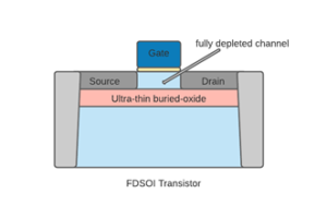
What is RF-SOI?
RF-SOI is name of a specialized semiconductor process utilized to create certain RF Integrated Circuits for applications like antenna tuners for cellphones and switching devices. Essentially, it is RF version of the SOI technology.
Historical Development and Evolution of RF-SOI Technology
Peregrine Semiconductor initiated
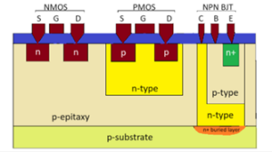
The semiconductor industry went through several stages of evolution, beginning with the Metal Oxide Semiconductor (MOS) Field-Effect Transistor (FET) which was first proposed by Lilienfeld and Heil in the 1930s, moving on to bipolar in the 1950s and N-channel metal-oxide semiconductor (NMOS) in 1970s, and ultimately becoming the standard in
Read More
BLOOMINGTON, Minn. – November 3, 2023 – SkyWater Technology (NASDAQ: SKYT), the trusted technology realization partner, today announced a new SkyWater open-source 130 nm process design kit (PDK) from Cadence Design Systems, Inc., which will be available in the Cadence® VLSI (very large-scale integration) Fundamentals Education Kit. The kit teaches students how theories and
Read More
SANTA CLARA, Calif., and MIGDAL HAEMEK, Israel, Sept. 5, 2023 – Intel Foundry Services (IFS) and Tower Semiconductor (Nasdaq: TSEM), a leading foundry for analog semiconductor solutions, today announced an agreement where Intel will provide foundry services and 300mm manufacturing capacity to
Read More
SAN JOSE, C.A., August 29, 2023 – At its annual Technology Summit beginning today, GlobalFoundries (GF) (Nasdaq: GFS), announced advancements in the industry’s first RFSOI foundry solution manufactured on 300mm wafers. Building upon its 8SW RFSOI technology and designed in collaboration with key customers, GF’s 9SW RFSOI technology is GF’s most advanced
Read More
July 5, 2023 — EUROPRACTICE Multi-Project Wafer (MPW) services will now offer flexible integrated circuit fabrication from Pragmatic Semiconductor, headquartered in Cambridge, UK. Within the EUROPRACTICE consortium, imec will be the partner that provides customers with access to Pragmatic’s technologies and technical support.
Pragmatic uses thin-film transistor (TFT) technology combined