


Despite an expected slowdown in growth this year and in 2020, the CMOS image sensor market is forecast to continue reaching record-high sales and unit volumes through 2023 with the spread of digital-imaging applications offsetting weakness in the global economy and the fallout from the U.S.-China trade war. CMOS image
Read More
Santa Clara, Calif. August 26, 2019 – GLOBALFOUNDRIES (GF), the world’s leading specialty foundry based in the United States, today filed multiple lawsuits in the U.S. and Germany alleging that semiconductor manufacturing technologies used by Taiwan Semiconductor Manufacturing Company Ltd. (TSMC) infringe 16 GF patents. The lawsuits were filed today in
Read More
Perceptia Devices, Inc. and GLOBALFOUNDRIES have agreed that Perceptia will join GLOBALFOUNDRIES in Santa Clara, California, on September 24, 2019, and in Munich, Germany, on October 11, 2019. GLOBALFOUNDRIES will hold its Technology Conference (GTC) in these locations, and Perceptia will be pleased to present its first three IPs available
Read More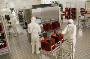
In the wake of tariffs and trade tension between China and the United States, government officials and company representatives throughout China have doubled down on their resolve to quickly and meaningfully grow the nation’s domestic IC business in order to reduce its dependence on critical IC components currently supplied by
Read More
China’s biggest semiconductor foundry is to withdraw from the New York Stock Exchange. SMIC notified the NYSE of its intention to apply on June 3 to delist its American depositary receipts (ADRs) from the bourse.
SMIC cited “a number of considerations,” including the limited trading volume of its ADSs
TSMC stands for Taiwan Semiconductor Manufacturing Company. TSMC, with its headquarters and primary operations located in Hsinchu Science Park in Taiwan, is the largest independent semiconductor foundry worldwide — making it a centerpiece in the world of fabless silicon manufacturing.
One cannot tell the story of TSMC without telling