


Vanguard International Semiconductor Corporation (VIS) and GLOBALFOUNDRIES (GF) today announced that VIS will acquire GF’s Fab 3E in Tampines, Singapore. The transaction includes buildings, facilities, and equipment, as well as IP associated with GF’s MEMS business. GF will continue to operate the facility through the end of 2019, providing a
Read More
IC Insights is in the process of completing its forecast and analysis of the IC industry and will present its new findings in The McClean Report 2019, which will be published later this month. Among the semiconductor industry data included in the new 400+ page report is an in-depth analysis of
Read More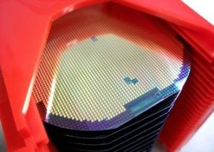
With the IC market on pace to surpass the $400 billion mark in 2018 after exceeding $300 billion just one year earlier, it is not surprising that fab capacity levels are on the rise too. A surge in new fab construction and existing fab upgrades is underway, but will it
Read More
The overall semiconductor equipment market is today worth several billion dollars. By contrast, the permanent bonding, temporary bonding and debonding and lithography equipment market for the MtM industry is a small niche representing millions of dollars. However, megatrend markets push MtM devices to new levels of complexity, resulting in big
Read More
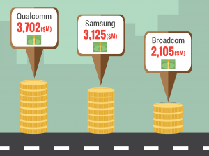
IC Insights revised its outlook for total semiconductor industry capital spending and presented its forecast of semiconductor capex spending for individual companies in its November Update to The McClean Report 2018, which was released earlier this month.
Samsung is expected to have the largest capex budget of any IC supplier again in
With tremendous growth of smartphones over the past decade, foundry sales to the communications market have soared and are now forecast to account for about 3x more than IC foundry sales to the computer market in 2018, based on IC Insights’ extensive part-two analysis of the integrated circuit foundry business
Read More