

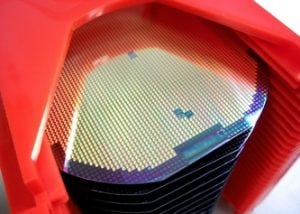
The average revenue generated from processed wafers among the four biggest pure-play foundries (TSMC, GlobalFoundries, UMC, and SMIC) is expected to be $1,138 in 2018, when expressed in 200mm-equivalent wafers, which is essentially flat from $1,136 in 2017, according to a new analysis by IC Insights (Figure 1). The average
Read More
IC Insights’ September Update to The McClean Report shows that as a result of a 51% forecasted increase in the China pure-play foundry market this year (Figure 1), China’s total share of the 2018 pure-play foundry market is expected to jump by five percentage points to 19%, exceeding the share held by the rest
Read More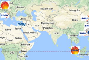
Wafer fabrication facilities, commonly known as wafer fabs, are the backbone of the semiconductor industry. These highly specialized factories process silicon wafers into integrated circuits (ICs) used in nearly every electronic device today. Let’s take a closer look at the global distribution and
Read More
GLOBALFOUNDRIES today announced an important step in its transformation, continuing the trajectory launched with the appointment of Tom Caulfield as CEO earlier this year. In line with the strategic direction Caulfield has articulated, GF is reshaping its technology portfolio to intensify its focus on delivering truly differentiated offerings for clients
Read More
Faraday Technology Corporation (TWSE: 3035), a leading ASIC design service and IP provider, today announced that it is leveraging Samsung FinFET platforms to extend its ASIC design solutions in next-generation applications, such as artificial intelligence (AI), 5G/infrastructure networking, blockchain, cloud storage, high-performance computing (HPC), AR & VR, and high-end imaging.
Read More
Synopsys, Inc. (Nasdaq: SNPS) today announced a collaboration with IBM to apply design technology co-optimization (DTCO) to the pathfinding of new semiconductor process technologies for the 3-nanometer (nm) process node and beyond. DTCO is a methodology for efficiently evaluating and down-selecting new transistor architectures, materials and other process technology innovations
Read More