


GLOBALFOUNDRIES today announced the signing of a memorandum of understanding to drive its next phase of growth in China. Through a joint venture with the government of Chongqing, the company plans to expand its global manufacturing footprint by establishing a 300mm fab in China. GLOBALFOUNDRIES is also investing in expanding
Read More
Researchers estimate that there are about 80,000 earthquakes globally each year, but most are too minor to notice. The Great East Japan Earthquake (a.k.a., 2011 Tohoku Earthquake) and subsequent tsunami that struck east of Sendai on March 11, 2011 caused substantial loss of life and destruction to infrastructure. It was
Read More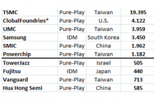
TSMC, by far, was the leader with $26.4 billion in sales last year. In fact, TSMC’s 2015 sales were over 5x that of second-ranked GlobalFoundries (even with the addition of IBM’s chip business in the second half of 2015) and almost 12x the sales of the fifth-ranked China-based foundry SMIC.
Read More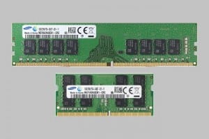
Samsung Electronics, the world leader in advanced memory technology, announced today that it has begun mass producing the industry’s first 10-nanometer (nm) class* , 8-gigabit (Gb) DDR4 (double-data-rate-4) DRAM chips and the modules derived from them. DDR4 is quickly becoming the most widely produced memory for personal computers and IT
Read More
TSMC, the world’s largest pure-play semiconductor foundry, plans to build a 12“ wafer fab a service center in Nanjing, China.
The new facility in China would be able to produce up to 20,000 12” wafers per month and will start production of 16-nanometer process technology in 2018, according to

Research in the field of 2D materials that started approximately five years ago, focusing on developing materials that are one layer thick which would make it faster for atoms to move in a single layer. Currently, transistors and other components used in electronic devices have been made of 3D materials
Read More