

Overview of Silicon-Germanium (SiGe) Technology and Historical Development
Shockley’s early transistor game most likely inspired the notion of fusing silicon (Si) and germanium (Ge) to create an alloy for use in transistor engineering. However, this concept has just become a reality in the last 15 years due to the challenges associated with producing lattice-matched Silicon-Germanium (SiGe) alloy atop Si. The main reason SiGe HBT technology failed to succeed in CMOS was its excessive power consumption. Originally, IBM developed SiGe HBT technology for the high-end computing industry [1].
IBM redirected its Silicon-Germanium (SiGe) development in the early 1990s to address the quickly expanding communications sector. It is interesting to note that SiGe HBT requires a lot less power than CMOS to function at the same level in RF communications circuits [2]. Considerable advancements have been made since then. Every significant telecommunications business has SiGe technology on its product roadmap, and it is being researched and deployed globally. High speed, high bandwidth instrumentation, disk storage, and wired and wireless communications circuits are only a few examples of applications. Wireless devices frequently use discrete SiGe HBTs and amplifiers. High-speed 10–40 Gb/s synchronous optical network (SONET) transceivers, wireless LAN chipsets, and GSM and CDMA wireless handsets and base stations all contain integrated Silicon-Germanium (SiGe) chips.
The idea of using silicon and germanium together in integrated circuits is not new. It is as old as the invention of transistor. Silicon Germanium bipolar complementary metal-oxide-semiconductor (SiGe BiCMOS) has become a dominant technology in the marketplace and continues to be used on a large scale for commercial integrated-circuit (IC) products. This technology has also displaced Gallium Arsenide (GaAs) and Indium Phosphide (InP) in many communication applications already. Most of the mobile phones, our global positioning system receivers (GPS), wireless local area networks (LAN) and TV tuners use SiGe BiCMOS for RF transmit and receive functions because of the above-mentioned advantages. Also, SiGe BiCMOS provides cost-effective solutions for challenging RF and complex analog circuit applications [3].
Composition and Properties of Silicon Germanium Alloys and SiGe HBTs
Silicon germanium (SiGe) alloys have attracted a lot of interest in semiconductor research because of their special structure and beneficial physical characteristics. SiGe alloys are preferable to their elemental equivalents because they can have adjustable properties due to their combination of germanium (Ge) and silicon (Si).
The atomistic structure of GeSi alloys is imperfect Pauling type, typical of disordered solids. As shown in Figure 1, the majority of the atomic strain in the alloys is accommodated by modifications to the alloy composition that affect both the link length and bond angle [4].
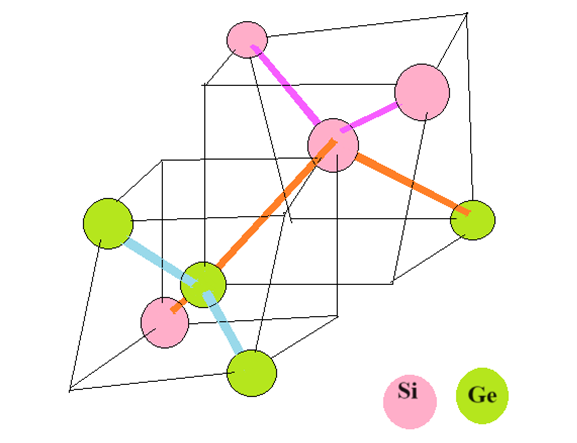
Figure 1. GeSi’s Local Atomistic Structure [4]
SiGe has better electron mobility than either pure silicon or germanium, which allows for better electrical performance. Higher carrier mobility is introduced by the addition of germanium to the silicon lattice structure, and this is essential for the advancement of high-speed electronic devices. Additionally, the alloy’s tunable bandgap enables customized electrical characteristics to meet particular application needs.
The composition of SiGe has a major impact on both its electrical and thermal performance. The effects of different concentrations of germanium on the properties of the alloy have been thoroughly investigated by researchers [5]. In general, higher germanium content increases carrier mobility, but it can also cause problems with thermal conductivity and crystal flaws. For SiGe to be implemented successfully in semiconductor devices, an ideal equilibrium must be reached.
Integrated circuits and SiGe heterojunction bipolar transistors (HBTs) are two popular applications for SiGe alloys. HBTs improve transistor performance by making use of the heterojunction interface between germanium and silicon, enabling quicker switching times and reduced power consumption. SiGe-based integrated circuits have shown excellent performance in high-frequency applications, which equips them for use in wireless and telecommunications networks.
—
Design and Fabrication Process of SiGe HBTs
In semiconductor engineering, the design and manufacturing of SiGe HBTs are essential to the field [6]. In order to create a heterojunction that improves electron mobility-a crucial component for attaining high-speed transistor operation-a thin SiGe layer is grown epitaxially on a silicon substrate to create SiGe HBTs [7]. Cutting-edge fabrication methods, like chemical vapor deposition and molecular beam epitaxy, provide exact control over layer composition and thickness, which is essential for customizing device performance.
A number of complex procedures are involved in the design and construction of SiGe HBTs in order to achieve exact control over the properties of the material and device performance. Semiconductor engineers may precisely design and fabricate SiGe HBTs and use their improved performance properties for a variety of high-frequency and high-speed applications by following the steps shown in Figure 2.
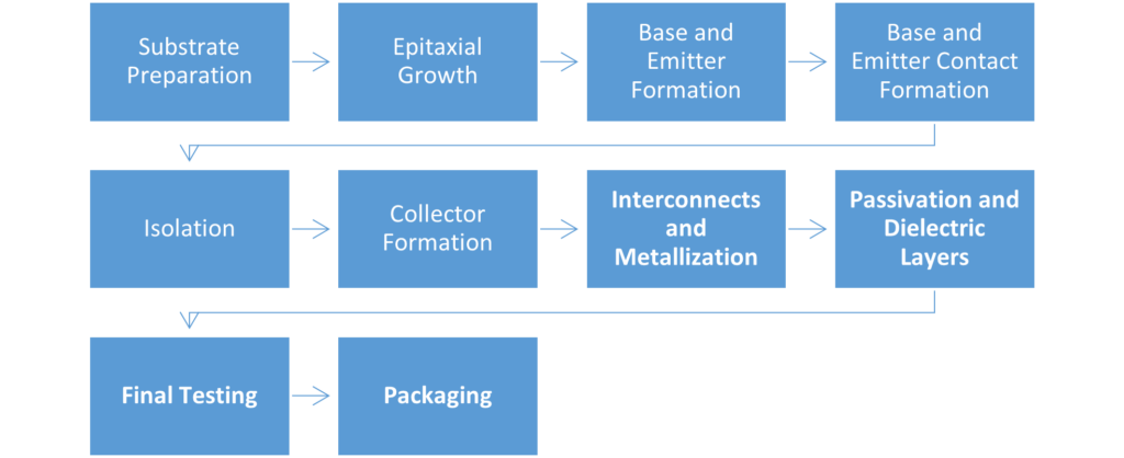
Figure 2. Design and Fabrication Steps of SiGe HBTs
Main Fabrication Process:
A typical cross section of a SiGe HBT [8] is shown in Figure 3 and the main fabrication process is as follow:
The shallow EB junction produced by the polysilicon region beneath the emitter lowers the parasitic EB capacitance [9].
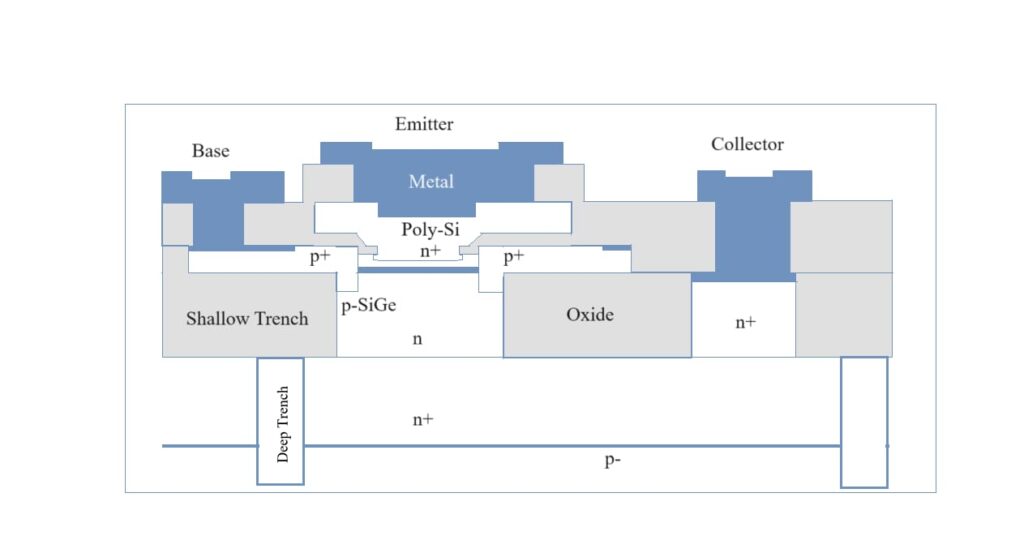
Figure 3. SiGe HBT Cross Sectional View
High-frequency and high-speed integrated circuits are the main applications for SiGe HBTs. These transistors work exceptionally well in microwave circuits, wireless communication systems, and RF applications. SiGe HBTs are essential parts in the design of due to their innate qualities of fast switching, low noise, and high-power gain.
High-Speed and Low-Power Capabilities in Wireless and Fiber-Optic Communications
The high-speed and low-power properties of SiGe technology make it essential for wireless and fiber-optic communications. Rapid data transmission is made possible by its excellent electron mobility and effective charge carrier injection, and communication systems’ energy efficiency is increased by its low power consumption.
SiGe RF ICs are being used in the communications, automotive, and navigation/aerospace industries. Figure 4 illustrates the SiGe frequency window of applications. SiGe has already seized a sizable share of the 2.4 GHz Bluetooth market. It has greater current gain, output conductance, temperature stability, and smaller noise margins than silicon. It also permits operating frequencies that are two to three times higher [10]. Phase-locked loops, power amplifiers (Pas), intermediate frequency mixers (IFs), voltage-controlled oscillators (VCOs), low noise amplifiers (LNAs), and analog-to-digital/digital-to-analog converters (ADC/DAC) are examples of analog components that use it.
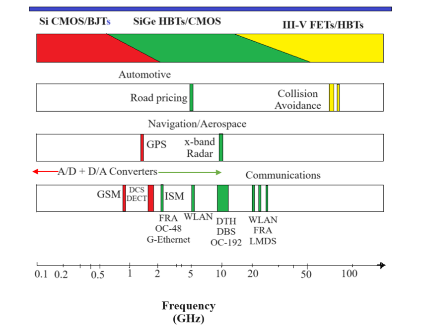
Figure 4. An Illustration of the Current SiGe Frequency Window of Applications
SiGe may find use in avalanche photo-diode photodetectors or optoelectronic superlattice structures in the future as its process technology advances and SiGe becomes more widely used. In an effort to facilitate the integration of GaAs-based devices onto silicon, researchers are looking at the use of SiGe as a pseudo-substrate for III-V compounds.
Thermal Management and Reliability Issues in SiGe Device Manufacturing
In the temperature range of 20°C to 700°C, the thermal conductivity, electrical conductivity, and Seebeck coefficient of high-quality crystals of Ge1-xSix alloys, both non- and Ga-doped in the entire composition 0 < x < 1, produced by the Czochralski technique, were examined [11]. The phonon scattering at point defects in an alloy semiconductor explains why the thermal resistivity was highly dependent on the alloy composition. Due to the drop in intrinsic carrier concentration caused by the band gap energy at high temperatures, the electrical conductivity decreased as x increased. It was found that the Ga-doped GeSi polycrystal with x = 0.81 had 400 uV/K at 600°C, while the Ga-doped GeSi single crystal with x = 0.95 had 200 uV/K at 600°C. Given the large ability of the GeSi alloys as a thermoelectric material, the figure of merit of the alloys was tested in [11] between 0.05 and 0.5.
Performance and Power Consumption Comparison of SiGe with other materials
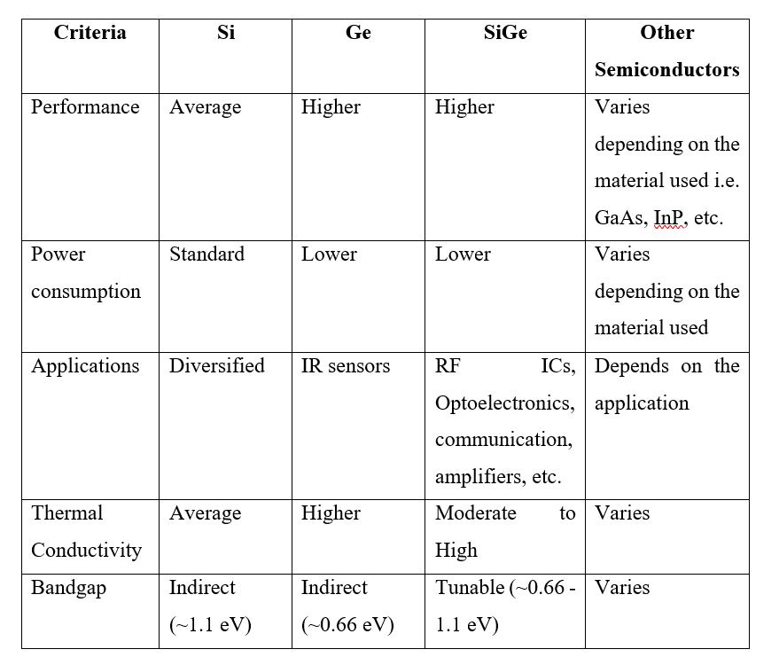
Table 1 compares SiGe to silicon, germanium, and other semiconductor materials in terms of performance, power consumption, and comparisons for certain applications.
Table 1. Comparison of SiGe with Silicon, Germanium, and other Semiconductor Materials [12]
Market Trends, Research Directions, and Adoption of SiGe Technology in Industry
Microcrystalline silicon germanium has been demonstrated in [13] to be a viable option for a bottom cell in a tandem junction device, which could lead to increased absorption at infrared wavelengths without lowering photon collection at lower wavelengths. Good crystallinity at different germanium concentrations in the c-Si1-xGex:H alloy could be obtained by using notably high hydrogen dilutions. The study was able to investigate the effects of the germanium content on several device parameters when these films were used as the foundation layers in a solar cell device. The diffusion length and minority carrier lifetime were evaluated simultaneously in these devices, and the hole mobility was calculated in [13].
An excitation frequency of 45MHz was utilized in a VHF PECVD reactor to deposit the c-Si1-xGex:H alloy in the study of [13]. 10% germane (the remainder being hydrogen), silane, and hydrogen were the gases used. The proportion of hydrogen to silane flow [H2]:[SiH4] was adjusted within a 25-30:1 range, whilst the flow of 10% germane [10%GeH4] was contingent upon the desired level of germanium incorporation in the alloy. Keep in mind that the ideal hydrogen dilution is determined by the quantity of germanium content in the films containing c-Si1-xGex:H higher hydrogen dilution needed for a higher germanium concentration to obtain high crystallinity. There was RF power limitation to the 30-35W range, and the pressure was maintained at 50 mT. The substrate is between 250 and 2750C in temperature.
The p+-n-n+ devices grew on substrates made of stainless steel without the need of a back reflector. Based on Figure 5, the structure is comprised of an intrinsic layer that is layered above an a-Si:H n+ bottom layer that is about 0.1 m thick. The base layer is composed of the actual c-Si1-xGex:H layer, a thin a-Si:H incubation layer (~20 nm thick), and a c-Si:H seed layer. Since the n-n+ interface is crucial for electron collection, the c-Si:H layer serves to maintain a smooth band gap fluctuation there and prevent any kinks in the conduction band. Similar to this, the germanium concentration is progressively lowered at the p+-n interface until the device ends with a c-Si:H p+ layer.
Because hole collection is lost with even little changes in band gap, this interface became challenging to engineer. The device is completed with a shattered ITO top contact. There were 0.6–0.7 m in the base layer.
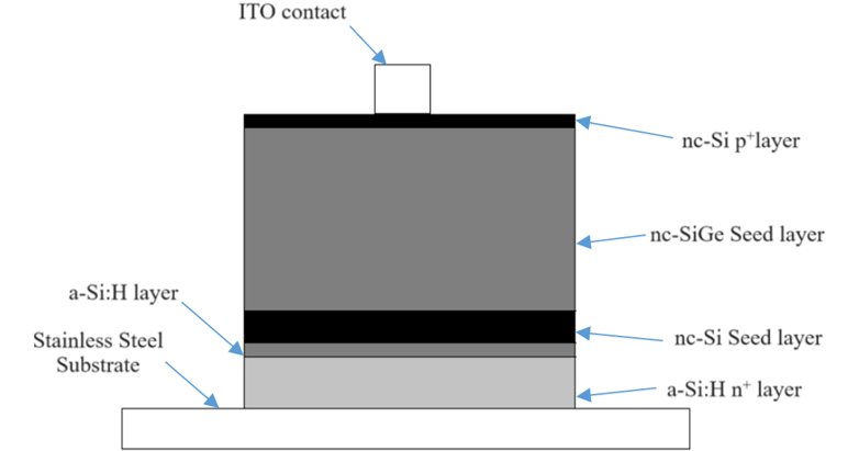
Figure 5: The growth of a simple solar cell on an untextured stainless steel substrate. For reference, different interface layers have names.
Current Trends and Role of SiGe Technology
With its enormous potential for high-speed data processing and communication, SiGe technology has established itself as a mainstay in the semiconductor sector. High-frequency and high-performance electronic devices have been made possible by recent breakthroughs in SiGe integration, which have also had a significant impact on major developments in semiconductor technology.
The use of SiGe technology in modern RF components is a noteworthy trend. By taking advantage of SiGe’s special qualities, high-speed transistors can be produced, opening the door to the development of extremely quick communication systems. This effect is especially noticeable in the telecom sector, where it makes 5G networks and other advanced technologies more feasible. The integration of SiGe has improved signal processing capabilities and has been crucial in the development of wireless connectivity, satellite communication, and radar systems.
Adoption And Developments In the Future
With current research focusing on extending the boundaries of SiGe integration, the prospects for SiGe technology seem bright. The goal is to reduce heat dissipation and increase power efficiency in order to meet the increasing demand for energy-efficient electronic equipment in a variety of applications.
Beyond conventional silicon-based methods, SiGe has evolved to provide technologies such as RF-SOI (Radio-Frequency Silicon-On-Insulator) and BiCMOS [14]. These developments have increased SiGe’s potential and increased its adaptability in semiconductor technology.
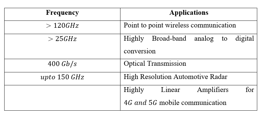
SiGe-BiCMOS technology finds its applications in millimeter-wave (mm-wave) and sub millimeter wave frequency spectrum [15]. Some of these applications are shown in Table 2.
Table 2. Applications of SiGe-BiCMOS Technology
Recent developments see SiGe integrated into advanced semiconductor processes, including FD-SOI (Fully Depleted Silicon-On-Insulator) technology [16]. FD-SOI enhances power efficiency and performance by utilizing a thin silicon layer on an insulating substrate, allowing better control over current flow, reducing leakage, and improving overall device efficiency. Additionally, SiGe is actively explored in heterogeneous integration, where different materials and technologies are combined on a single chip, optimizing performance and leading to more compact and efficient electronic systems.
References:
[1] Harame, David L., and Bernard S. Meyerson. “The early history of IBM’s SiGe mixed signal technology.” IEEE Transactions on Electron Devices 48, no. 11 (2001): 2555-2567.
[2] Niu, Guofu. “SiGe Technology for Revolution of Personal Communications.” online resources: http://www. eng. aubum. edu/users/niuguof/sige_intro. htm (2002).
[3] Phillips, S., Ed Preisler, J. Zheng, S. Chaudhry, M. Racanelli, M. Müller, Michael Schröter, W. McArthur, and D. Howard. “Advances in foundry SiGe HBT BiCMOS processes through modeling and device scaling for ultra-high speed applications.” In 2021 IEEE BiCMOS and Compound Semiconductor Integrated Circuits and Technology Symposium (BCICTS), pp. 1-5. IEEE, 2021.
[4] Yonenaga, Ichiro, and M. Sakurai. “Bond lengths in Ge 1− x Si x crystalline alloys grown by the Czochralski method.” Physical Review B 64, no. 11 (2001): 113206.
[5] Sereni, Julian Gustavo Renzo. “Reference module in materials science and materials engineering.” (2016).
[6] Sumei, Jia, and Yang Ruixia. “The Research on Process Technology of SiGe/Si HBT.” Procedia Engineering 15 (2011): 4021-4025.
[7] Mitchell, Gregory A. The Role of the Silicon Germanium (SiGe) Heterojunction Bipolar Transistor (HBT) in Mobile Technology Platforms. Army Research Laboratory, 2011.
[8] Cressler, J; Niu, Guofu. Silicon-Germanium Heterojunction Bipolar Transistors; Artech House Inc: Boston, MA, 2003.
[9] Ashburn, P. SiGe Heterojunction Bipolar Transistors; John Wiley & Sons, LTD: West Sussex, England, 2003.
[10]https://www.rfglobalnet.com/doc/sisige-devices-and-the-rf-communications-revo-0001#:~:text=These%20SiGe%20RF%20BiCMOS%20chips,wireless%20communication%20links%20to%20networks.&text=SiGe%20RF%20ICs%20are%20finding,Bluetooth%20(2.4%20GHz)%20market.
[11] Yonenaga, I., T. Goto, X. F. Tang, and S. Yamaguchi. “Thermal and electrical properties of Czochralski grown germanium-silicon alloys.” In Eighteenth International Conference on Thermoelectrics. Proceedings, ICT’99 (Cat. No. 99TH8407), pp. 436-439. IEEE, 1999.
[12] Haddara, Yaser M., Peter Ashburn, and Darren M. Bagnall. “Silicon-germanium: properties, growth and applications.” Springer handbook of electronic and photonic materials (2017): 1-1.
[13] Saripalli, Satya, and Vikram Dalal. “Microcrystalline silicon-germanium solar cells fabricated using VHF PECVD.” In 2008 IEEE International Conference on Electro/Information Technology, pp. 414-418. IEEE, 2008.
[14] Du Preez, Jaco, Saurabh Sinha, and Kaushik Sengupta. “SiGe and CMOS Technology for State-of-the-Art Millimeter-Wave Transceivers.” IEEE Access (2023).
[15] Zimmer, Thomas, Josef Böck, Fred Buchali, Pascal Chevalier, Michael Collisi, Björn Debaillie, Marina Deng et al. “SiGe HBTs and BiCMOS technology for present and future millimeter-wave systems.” IEEE Journal of Microwaves 1, no. 1 (2021): 288-298.
[16] Gatzastras, Athanasios, Christian Volmer, and Ingmar Kallfass. “A Fully-Differential Travelling-Wave Amplifier up to 110 GHz in a 22 nm FD-SOI CMOS Technology.” In 2023 18th European Microwave Integrated Circuits Conference (EuMIC), pp. 365-368. IEEE, 2023.
