
On the evening of Saturday, March 21, 2026, Elon Musk took the stage at the defunct Seaholm Power Plant in Austin, Texas, and made what may be the most audacious announcement of his career — and that is saying something. Standing before a crowd of investors, engineers, and cameras streaming live on X, he unveiled Terafab: a joint $20–25 billion semiconductor fabrication facility that he described as “the most epic chip building exercise in history by far.” Texas Governor Greg Abbott was in the audience. Light beams shot into the Austin sky. The spectacle was unmistakably Musk.
The bold rhetoric was vintage. The ambition behind it, however, is unprecedented — even by his standards.
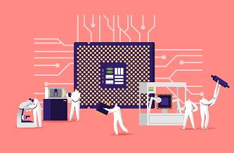
Terafab is a joint venture between three of Musk’s companies: Tesla, SpaceX, and xAI — the AI startup SpaceX acquired in an all-stock deal earlier in 2026. The facility is designed to consolidate the entire semiconductor manufacturing value chain under one roof: chip design, lithography, fabrication, memory production, advanced packaging, and final testing. In the semiconductor world, this kind of full-stack vertical integration simply does not exist anywhere else on the planet.
The technology target is equally aggressive. Musk says Terafab will produce chips at the 2-nanometer process node — the most advanced level of fabrication currently entering commercial production. At the time of announcement, only TSMC was capable of manufacturing 2nm chips, a capability built over decades and hundreds of billions of dollars of investment. Terafab’s two product lines reflect the breadth of the venture: inference chips for Tesla vehicles and Optimus humanoid robots, and space-grade D3 chips engineered to withstand the thermal and radiation demands of orbital deployment.
The location is confirmed. Construction is already underway on the North Campus of Giga Texas, Tesla’s existing manufacturing complex in eastern Travis County, near Austin — and the site activity visible from the air tells a story the announcement confirmed.
Aerial observer Joe Tegtmeyer, who has tracked the Giga Texas campus for years via drone footage, documented extensive ground clearing, soil reclamation, and infill operations on land that sits outside Tesla’s existing property boundary — meaning the company has quietly acquired adjacent terrain specifically for this expansion. His estimates place the basic footprint at approximately 2 million square feet, though the final production area could climb significantly higher if the facility goes multi-story, as expected. Permit documents now circulating indicate Tesla is seeking to add over 5.2 million square feet of new building space to the Giga Texas campus by the end of 2026 alone.
Bloomberg reported that Musk confirmed the project will begin with a smaller “advanced technology fab” in Austin — housing all the equipment needed to make and test chips of any kind — before scaling toward the full Terafab vision. The phased approach is a tacit acknowledgment of the complexity involved. Even so, the construction groundwork suggests Tesla is past the drawing board and into the dirt.
Musk’s production targets are staggering. He says Terafab will begin operations at 100,000 wafer starts per month, scaling ultimately to 1 million wafer starts per month at full capacity. That final figure would represent roughly 70% of TSMC’s entire current global output — from a single facility operated by companies that have never fabricated a chip in their lives.
The annual compute output goal is equally eye-watering: 1 terawatt of computing power per year, a number that gives the project its name. To achieve this, Terafab would need to produce between 100 and 200 billion custom AI and memory chips annually, powering everything from Tesla’s Full Self-Driving system and Optimus humanoid robots to xAI’s Grok and a planned network of orbital AI satellites.
The cost estimate of $20–25 billion is itself a figure worth pausing on. Tesla’s CFO acknowledged that this sum is not yet incorporated into Tesla’s capital expenditure plan for 2026 — which already exceeds $20 billion on its own.
The rationale Musk offered for Terafab is rooted in a supply chain argument he has been building for over a year. At Tesla’s Q4 2025 earnings call, he warned investors that external chip capacity from TSMC, Samsung, and Micron would hit a ceiling within three to four years, long before his demand projections for Optimus robots, autonomous vehicles, and AI data centers could be met.
“We either build the Terafab or we don’t have the chips,” Musk said at the launch event. He acknowledged his current suppliers — thanking TSMC, Samsung, and Micron — but argued there is a “maximum rate at which they’re comfortable expanding.” For a company projecting the chip volumes needed to field millions of humanoid robots and autonomous vehicles simultaneously, that ceiling arrives uncomfortably fast.
The space dimension of the announcement adds another layer. Musk said that roughly 80% of Terafab’s compute output would eventually be directed toward space-based orbital AI satellites, arguing that solar irradiance in orbit is roughly five times greater than at Earth’s surface, and that heat dissipation in the vacuum of space makes thermal scaling far more viable than in terrestrial data centers.
This is where Terafab faces its steepest climb — and where the gap between vision and reality is most exposed. The technology stack has several layers, each with its own formidable constraints.
Lithography: The ASML Bottleneck
To manufacture chips at 2nm, Terafab would need High-NA EUV (Extreme Ultraviolet) lithography machines from ASML — the Dutch company that is, quite literally, the only supplier of these systems in the world. Each machine carries a price tag of roughly $370–400 million, and ASML’s order books are already under extreme pressure. ASML’s Q4 2025 orders doubled analyst expectations, and its 2026 revenue guidance reflects a global queue of customers that includes TSMC, Samsung, and Intel. Securing enough EUV machines on a timeline that supports even a 2028 production start would require placing orders immediately — and even then, delivery is not guaranteed.
Process Knowledge: The Samsung Bridge
Tesla is not trying to reinvent semiconductor process technology from scratch. Instead, the company has already signed a $16.5 billion multi-year contract with Samsung for the manufacture of its next-generation AI6 chips at U.S.-based Samsung fabs. Analysts view this Samsung relationship as a critical knowledge bridge — a way for Tesla engineers to absorb institutional familiarity with leading-edge fab processes before attempting to run their own. The arrangement creates an awkward dynamic for Samsung: it benefits in the near term from a major Tesla order, while simultaneously risking the emergence of a well-capitalised future competitor.
Talent: Hiring From Zero
Building a fab is not just about pouring concrete and ordering machines — it requires a workforce of highly specialized process engineers covering lithography, etching, chemical-mechanical planarization, yield management, and EUV equipment operation. These are disciplines Tesla has never employed. The company has already posted job listings for a Technical Program Manager in Infrastructure Semiconductors in Austin, requiring 10+ years of program management experience, 5+ years in semiconductor or high-tech manufacturing, and a track record leading projects with over $100 million in capital expenditure. These are extraordinarily rare profiles, and the postings signal that Tesla is still in the late planning stage — not yet at final investment decision.
Musk’s Unconventional Cleanroom Theory
Perhaps the most eyebrow-raising technology claim is Musk’s contention that the semiconductor industry has been building cleanrooms wrong for decades. Modern leading-edge fabs operate at ISO Class 1–3 cleanroom standards — environments so sterile that a single human breath can introduce enough contamination to ruin chips at the nanometer scale. Musk has argued that Terafab’s wafers will be fully enclosed at all times, theoretically eliminating the need for a traditional cleanroom environment. It is a theory that, if proven, would be genuinely revolutionary. It has also never been demonstrated at any scale.
The semiconductor industry did not greet the Terafab announcement with universal applause. Jensen Huang, Nvidia’s CEO and one of the most informed voices on chip supply chains alive, issued a pointed public warning months before the launch: “Building advanced chip manufacturing is extremely hard. It is not just build the plant, but the engineering, the science, and the artistry of doing what TSMC does for a living is extremely hard.” He told reporters that matching TSMC’s capabilities is “virtually impossible” — notable given that Huang has every incentive to want more chip production capacity in the world.
Tesla’s lack of institutional knowledge in semiconductor manufacturing remains the sharpest critique. While the company did build a capable chip design team — hiring legends like Jim Keller and later Peter Bannon from Apple — much of that talent has since departed. Bannon, Tesla’s head of custom silicon, left in August 2025, the same month Musk cancelled the entire Dojo supercomputer program. Chip design and chip fabrication are entirely different disciplines, and the knowledge gap is vast.
Critics have also drawn a direct parallel to Tesla’s Battery Day in September 2020, when Musk promised a revolution in 4680 battery cell manufacturing. Five and a half years later, the program has delivered far less than promised, with delayed timelines, revised processes, and production targets that remain a distant reality. The pattern is hard to ignore.
Analysts at major investment banks have described Terafab as Tesla’s “most Herculean task ever,” suggesting that even under an aggressive scenario, initial chip output would not occur until mid-2028 at the earliest.
Whatever the final outcome, Terafab has already accomplished something significant: it has forced the global semiconductor industry to take Musk’s supply chain ambitions seriously. Whether the facility ever reaches 1 million wafers per month or not, the announcement signals that one of the world’s largest consumers of AI compute is no longer willing to remain dependent on external foundries.
The geopolitical timing is notable. With TSMC’s dominance concentrated in Taiwan, growing U.S.–China tensions, and a wave of domestic semiconductor investment incentivized by the CHIPS Act, a large-scale American-owned fab in Austin fits neatly into a broader industrial policy narrative. Governor Abbott’s presence at the launch was not incidental.
Elon Musk has a well-documented pattern of promising the extraordinary and delivering something that, while often late and smaller than claimed, still shifts the underlying landscape. Whether Terafab will join that tradition — or become the most expensive lesson in semiconductor humility ever recorded — is a question the chip industry will be watching very closely.