

Semiconductor foundries claim they release a new technology node every two years. They may be off by a year or two, but on the whole, this is quite impressive, no doubt. Come to think of it, I don’t believe many of us even change our mobile phone every two years. How about ASIC developers – can they keep up with this pace? How long do semiconductor technology nodes remain and when do companies switch?
Let’s take a look at the semiconductor technology node history, analyze the trends and try to forecast the near future.
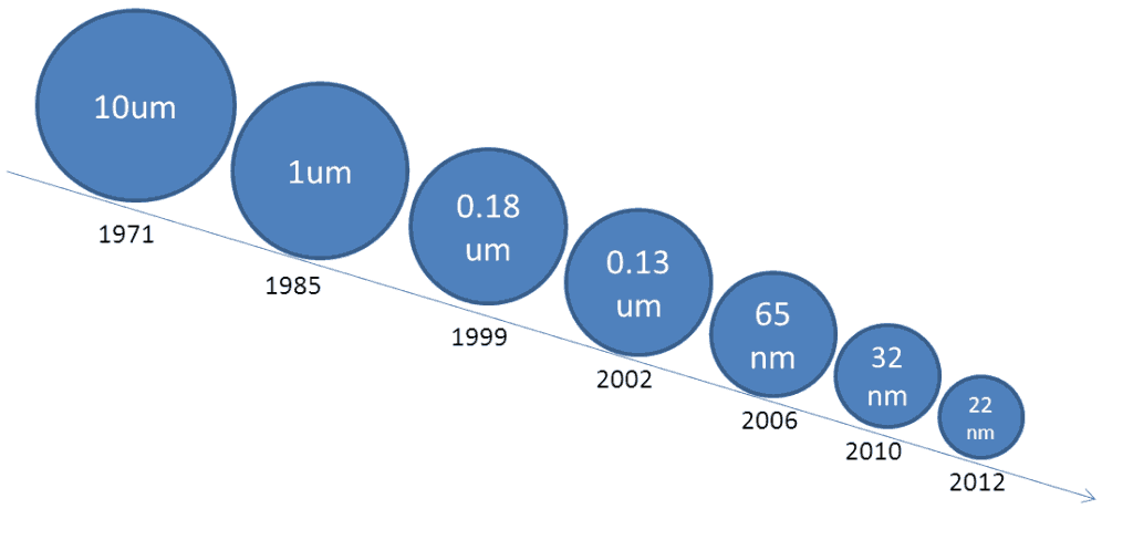
Many years before TSMC, GLOBALFOUNDRIES and other foundries existed, the very first commercial technology node was 10um. Today it may seem irrelevant, but in 1971 Intel gave birth to the first CPU using this technology. At that time, a technology node at this geometry was state-of-the-art. It was highly complex, not only because of the new breakthrough technology but also because the EDA market was not there yet to support the poor engineers with useful software tools.
Today, there is a huge variety of semiconductor foundries (100+), technologies, technology nodes and flavors. Some technology nodes are more successful than others and other “classic” technology nodes are still appreciated and used even today. Not all applications need the performance of FinFET transistors at 28nm. Many are happy with an old-fashion 0.18um technology. Surprisingly enough, and based on figures we provide in this article, the number of 0.18um tape-outs is quite high – double the number of 90nm tape-outs.
Obviously, there is a limited life time to each technology and no technology node will last forever. Just like the 10um technology node phased out many years ago, the more advanced technologies of today will follow this path and discontinue.
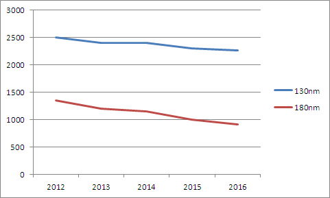
Overall, there are still many tape-outs using 0.18um and 0.13um, though the overall the number is declining.
The analog/mixed signal market is still very active in the mature technologies space and does not have a compelling reason to jump to advanced semiconductor technologies. The analog blocks will not scale with advanced nodes and therefore no significant die size reduction will be achieved. For the analog designer these semiconductor technologies are ideal –mature, robust, low cost and easy to use.
With mixed signal designs, things are a bit different. In many new mixed signal designs, digital blocks are becoming larger than the analog blocks. In such cases, and particularly in consumer electronics projects, customers will consider jumping to the deep submicron technologies to benefit from cost reduction.
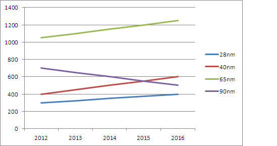
Today it would probably be safe to assert that the 90nm technology node (200mm wafer size) was not so successful, and therefore predict that the number of tape-outs using this node will continue to drop.
In the small geometries, 65nm technology node is in the leader in terms of new tape-outs. We can already notice that 28nm and 40nm are starting to have a good response from the market. 28nm, which is a relatively new technology, will continue to add approximately ~50 new tape-outs year to year. 40nm will add ~100 new tape-outs from year to year.
One of the biggest barriers of starting new designs in 65nn and below is the extremely high mask set cost. Many customers simply cannot afford the costs of deep submicron technology.
—
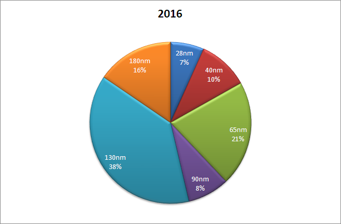
In the mature technology space (0.18um-0.13um), 0.13um will be the technology of choice for most applications. We predict that 0.13um technology will still remain dominant with more than 2000 tape outs in 2016. 0.13um node will have longer life time than 0.18um and will offer a more attractive cost structure.
In the deep submicron market, the number of tape-outs in 90nm will continue dropping, while 40nm and 28nm will become more attractive to new projects that require either low power properties or high performance computing.
For conventional digital project customers will use 65nm instead of 130nm and we will see this trend develop very soon. The prices of 65nm maskset and wafers are dropping and becoming more accessible to a wider set of applications.


