

Understanding the semiconductor manufacturing process is essential to appreciate the significance of BEOL. Semiconductor production is typically divided into three main phases: Front End of Line (FEOL), Middle End of Line (MEOL), and Back End of Line (BEOL). While FEOL focuses on building transistors and MEOL facilitates their connections, BEOL is responsible for providing the finishing touches that ensure devices perform optimally and reliably.
In this article, we will explore the critical role of BEOL in semiconductor production, delving into the key processes such as metallization and the formation of conductive interconnects. We’ll uncover the unique challenges faced during this phase, as well as the innovative solutions and trends shaping the future of BEOL technology.
The semiconductor manufacturing process is a complex series of steps used to create integrated circuits found in many electronic devices. This intricate process involves several stages, each crucial for the development of chips used in computers, smartphones, and more. The process focuses largely on building electrical properties and fine-tuning layers, crucial for the performance and longevity of electronic devices. Nanotechnologies and advanced materials play a significant role in enhancing the functionality of these electronic components. Understanding this process provides insight into the technological advancements that drive the modern digital world. Each step is vital, contributing to the overall efficiency and capability of integrated circuits.
Source: Wikipedia
Overview of Semiconductor Manufacturing
Semiconductor manufacturing is the backbone of the electronics industry, producing essential components like integrated circuits. This complex process involves the careful layering and patterning of materials on a silicon wafer. A crucial part of this process is the deposition of metal layers, which form the intricate pathways for electrical signals. Layers of silicon dioxide and other materials provide the necessary protective layers and support. As technology advances, the integration of nanotechnologies and three-dimensional integration techniques allows for more powerful and efficient devices. The careful balance of these elements ensures the production of reliable and efficient electronic components.
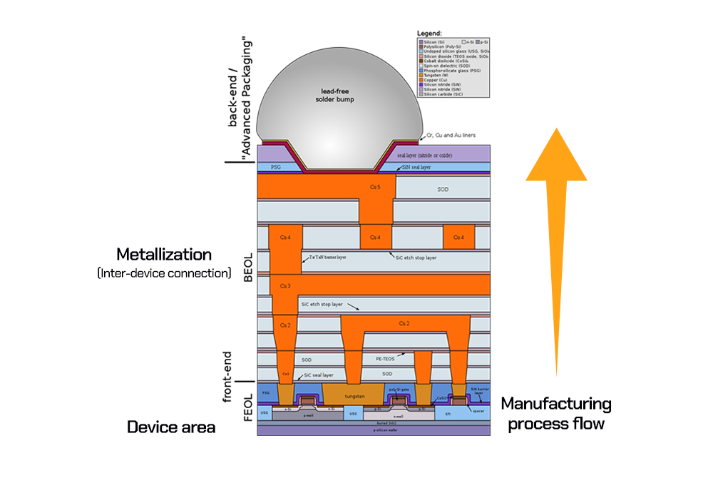
Difference Between FEOL, MEOL, and BEOL
The semiconductor manufacturing process is divided into several stages, namely Front-End Of Line (FEOL), Middle-End Of Line (MEOL), and Back-End Of Line (BEOL). Each stage serves a unique purpose in chip production.
Front-End Of Line (FEOL): FEOL refers to the initial phase where transistors are built within the wafer. This phase focuses on the formation of electrical properties, ensuring that the transistors can control electrical signals effectively. The integration of accurate doping and ion transport is crucial here.
Middle-End Of Line (MEOL): MEOL connects FEOL-created transistors to the metal layers applied in the BEOL process. This stage includes forming vias or small openings that link the layers together, crucial for the integration of individual chips into a compatible memory array.
Back-End Of Line (BEOL): BEOL involves the addition of metal layers that create the conductive paths for electrical signals on the chip. This stage often uses materials and techniques like atomic layer deposition and hybrid bonding to enhance thermal resistance and manage the chip for packaging in electronic devices. Advanced processes, like extreme ultraviolet lithography, are also used to perfect the intricate structures fabricated during this phase. The BEOL step ensures that chips function seamlessly within broader electronic systems.
The Back End of Line (BEOL) is a vital phase in semiconductor manufacturing. This part of the process involves creating metal layers and electrical pathways. These components are crucial for completing integrated circuits and ensuring electronic devices function correctly. BEOL follows the Front End of Line (FEOL), which deals with building the transistors on a chip. Its focus is on connecting these transistors and forming electrical signals to drive device functionality. By using techniques such as atomic layer deposition, manufacturers achieve precise control over chip components, which is crucial for supporting nanotechnologies for computing.
Importance of BEOL in Device Functionality
The BEOL process is essential for establishing the electrical properties needed for semiconductor devices. It involves depositing protective layers, such as a layer of silicon dioxide, which protect and insulate the delicate components on the chip. This phase also includes creating a three-dimensional integration of structures that allow for improved thermal resistance and hybrid bonding. Such integration enhances how individual chips function within larger systems, maintaining essential site functionality. Without BEOL, chips would lack the necessary infrastructure to connect and communicate effectively. Thus, BEOL not only supports the integration of complex tasks but also ensures that devices are powerful and efficient.
Impact of BEOL on Performance and Reliability
The BEOL stage greatly affects a chip’s performance and reliability. It ensures that electrical signals travel without interruption and that chip for packaging components are durable over time. The complex process of adding metal layers and protective coatings helps in minimizing potential failures. By enhancing thermal resistance and providing stable pathways for electrical conduction, BEOL extends the lifespan of electronic devices. Furthermore, the careful integration of nanotechnologies at this stage enhances the memory array’s compatibility, leading to better performance in demanding applications. The emphasis on precision in BEOL processes plays a critical role in the semiconductor industry, influencing every device’s overall effectiveness, from sensors to processors.
The Back End of Line (BEOL) is a critical stage in the semiconductor manufacturing process. It involves various methods and technologies to finalize the creation of integrated circuits. This phase focuses on layering and connecting components on the chip. These tasks are vital because they directly affect the chip’s performance and reliability. By ensuring proper connections and protecting the chip, BEOL adds the finishing touches to a complex process. The BEOL includes several key steps, such as the metallization process, formation of conductive interconnects, applying passivation layers, and final testing. Each of these steps plays a significant role in producing efficient and robust electronic devices.
Metallization Process
The metallization process is a core part of semiconductor manufacturing in the BEOL phase. In this step, metal layers are added to the chip to create pathways for electrical signals. These layers connect various components within the integrated circuit. The process typically involves techniques such as sputtering and atomic layer deposition to ensure thin, uniform coatings. The aim is to provide excellent electrical conductivity while maintaining the device’s mechanical integrity. The choice of metals, like copper or aluminum, is crucial because it influences the chip’s thermal resistance and electrical properties. Advanced technologies integrate these metals with other nanotechnologies for enhanced performance.
Formation of Conductive Interconnects
Conductive interconnects are essential for connecting different parts of an integrated circuit. These interconnects allow electrical signals to travel swiftly and efficiently across the chip. Their formation is a multi-step process involving the precise deposition of metal lines. This is usually achieved through methods like lithography and etching. The interconnects must be carefully designed to minimize resistance, which can otherwise lead to heat accumulation and slower signal transmission. High-quality interconnects are pivotal for the chip’s speed and functionality. As chips become more complex, three-dimensional integration may be employed, where interconnects link individual chips stacked within a device, promoting improved communication and better space usage.
Application of Passivation Layers
The application of passivation layers serves as a protective measure for integrated circuits. These layers are made of materials like silicon dioxide and silicon nitride. They are used to shield the delicate components of a chip from environmental contaminants such as moisture and chemicals. The passivation layer also helps in preventing mechanical damage and electrical interference. Implementing these layers is critical in ensuring the long-term reliability and stability of electronic devices. Besides providing protection, these layers must be compatible with the metal layers and other materials used during the manufacturing process. This compatibility ensures seamless integration and reduces the risk of performance issues or failures.
Final Testing and Quality Assurance
Final testing and quality assurance are the concluding steps in the BEOL phase. After the integration of various components and protective layers, each chip undergoes rigorous testing. This process ensures that every aspect of the chip meets quality standards for functionality and performance. Tests are conducted to check electrical properties, thermal resistance, and overall durability. The quality checks help in identifying defects and ensuring that the chips operate as intended in diverse conditions. This stage also involves confirming that chips will perform correctly within their intended applications, such as computing or advanced electronics. The comprehensive quality assurance process guarantees that the end products are reliable and efficient before being packaged and delivered to consumers.
The back end of line (BEOL) is a crucial step in the semiconductor manufacturing process. It involves adding several metal layers to connect individual components within integrated circuits. This process is essential for building electronic devices with efficient electrical properties. However, the BEOL faces several challenges that must be addressed to enhance the performance and durability of these components. These challenges often arise due to the integration of nanotechnologies and the need for three-dimensional integration in modern chips. This section will explore solutions to these issues, focusing on scaling challenges, improving yield, and enhancing overall device durability.
Addressing Scaling Challenges
As the demand for smaller and more powerful electronic devices grows, scaling the BEOL process becomes increasingly challenging. Shrinking the components requires precise control over protective layers like silicon dioxide and the metal deposition process. Atomic layer deposition techniques help achieve the required precision by adding materials one atomic layer at a time. This method ensures accurate placement and thickness control, essential for maintaining electrical signals within small spaces. Using extreme ultraviolet (EUV) lithography allows for more precise patterning, enabling further miniaturization of components. These advancements help address scaling challenges and facilitate the successful integration of nanotechnologies for computing.
Techniques for Improving Yield
Improving the yield of semiconductor manufacturing processes is vital for cost efficiency. Yield refers to the number of functional chips produced from a manufacturing batch. To enhance yield, manufacturers employ advanced techniques, including hybrid bonding and improved deposition processes. Hybrid bonding connects individual chips, enhancing functionality while maintaining thermal resistance. Tight process control is crucial for the deposition of metal layers. Ensuring uniformity during these phases reduces the likelihood of defects, which can impair the electrical properties of integrated circuits. Furthermore, refining the integration process of nanotechnology aids in achieving higher yield rates in semiconductor production.
Enhancing Overall Device Durability
Device durability is essential for ensuring the longevity and reliable function of electronic devices. Protective layers, such as those made from silicon dioxide, shield critical components from environmental damage and electrical interference. The semiconductor industry continuously explores new materials and methods to enhance durability. Advanced techniques focus on improving the chip packaging, which plays a significant role in protecting the components. Techniques like hybrid bonding contribute to structural stability, ensuring that these devices can endure complex tasks without performance degradation. By focusing on these areas, semiconductor manufacturers aim to produce resilient devices capable of withstanding harsh conditions and extended use.
Innovations and Trends in BEOL
The Back End of Line (BEOL) in semiconductor manufacturing plays a crucial role in the overall performance of electronic devices. It involves complex processes that connect different parts of integrated circuits. The BEOL focuses on completing the circuit patterns on individual chips through various deposition processes. Recent innovations are transforming how these processes take place, with trends pointing towards more efficient and reliable solutions. With advancements in areas like metallization techniques and the use of new materials, BEOL processes are becoming more integral to achieving higher performance in computing devices. Let’s explore these trends and innovations that are shaping the future of BEOL.
Advances in Metallization Techniques
Metallization is essential for creating the metal layers that interconnect different parts of integrated circuits. Advances in this area focus on improving electrical properties and reliability. New metallization techniques aim to improve electrical signals while reducing resistance and capacitance. This ensures faster and more efficient chip performance. Hybrid bonding is one such technique gaining traction. It involves creating three-dimensional integration which enhances chip packaging. These techniques are designed to improve the thermal resistance of electronic devices, ensuring they can handle higher power outputs without overheating. As technology demands grow, metallization techniques continue to evolve to meet these challenges in the semiconductor industry.
New Materials in BEOL Processes
The use of new materials in BEOL processes is revolutionizing how integrated circuits are manufactured. One focus area is the integration of nanotechnologies, which allows for more precise and smaller circuit patterns. Advanced materials like atomic layer deposition are being explored to create protective layers that improve chip reliability. Additionally, using materials such as a layer of silicon dioxide helps enhance the electrical and thermal properties of chips. These materials are chosen for their compatibility with existing processes and their ability to offer better performance metrics. As the industry pushes towards miniaturization, these materials become essential in achieving cutting-edge performance and efficiency.
Automation and Precision Technologies
Automation is transforming BEOL by increasing efficiency and precision. With complex tasks involved in the semiconductor manufacturing process, automation ensures that each step is carried out with precision. Technologies that offer extreme ultraviolet lithography are enabling more detailed and smaller feature sizes on chips. Automation reduces errors and increases the speed of production, crucial for meeting the demand for advanced computing devices. Precision technologies are being integrated into existing processes to enhance essential site functionality. As the semiconductor industry evolves, automation becomes a pivotal factor ensuring that devices meet the growing needs for computational power and speed.


