Burn in sockets a pivotal role in stress-testing ASIC chips, helping manufacturers identify early failures and improve product quality. These sockets are IC burn in sockets that are used in ASIC accelerated stress tests to conduct burn in testing, therefore they are design to withstand high temperature conditions.
A burn-in socket is an essential component in the qualification process for an ASIC or SoC . It’s designed to facilitate burn-in testing, which involves operating a device at elevated temperatures— ASIC Qualification (for example: HTOL: High Temperature Operating Life) — to accelerate failure mechanisms and ensure long-term reliability.
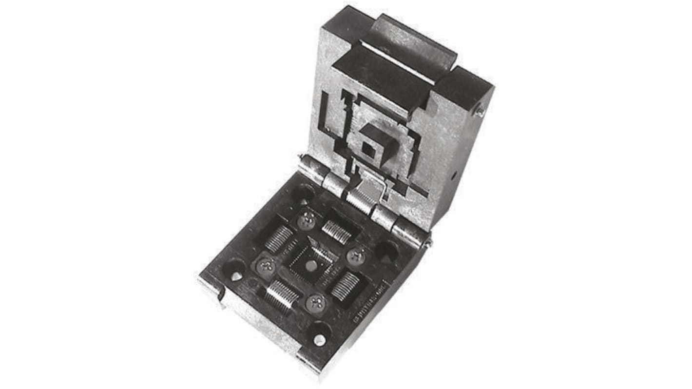
Compliant with JEDEC standards, burn-in sockets are crucial for temperature testing, as they provide both the physical and electrical interface between the device under test (DUT) and the burn-in board. With various socket designs available, including open-top and Ball Grid Array (BGA) sockets, they cater to a range of package sizes and product types.
The body of a burn-in socket is crafted to withstand high-temperature environments and to provide consistent connectivity.
In essence, burn-in sockets are tailored to meet the rigorous testing requirements of the semiconductor industry.
When selecting a burn-in socket for electronic device testing, multiple factors must be accounted for to ensure optimal performance and compatibility:
In summary, the right burn-in socket maximizes efficiency and accuracy during the testing phase, catering to specific device types, industry standards, and testing conditions.