

Many IC designers pay little attention to ASIC qualification and consequently pay high price and delays before the chip reaches to high volume. The mindset of experienced IC designers is considering IC quality (and reliability) through all phases of the IC design process. Today, more than ever, re-tapeout is costly and can be very painful for startup fabless companies. This guide will help you with understanding the setting up an ASIC qualification plan for your semiconductor device.

Download the full image “IC Qualification JEDEC Overview” here.
Before setting an IC qualification plan, it is recommended that you gather inputs from your customer regarding the normal operating conditions for the IC as well as their target requirements for the quality and reliability. Typically, this information is generally not easy obtain, especially for the start-up fabless company. A mature fabless company that has provided a number of ASIC to the same customer should have access to such information.
IC quality level is determined by the target market: consumer, space, automotive etc. Each market has its own reliability and quality requirements. It’s advised to check the required quality level by conducting customer interviews. Some customers will have stringent quality requirements therefore you will have to conduct longer and more comprehensive ASIC qualification tests.
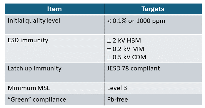
In the absence any customer requirements, it is recommended to the generally accepted numbers from JEDEC standards. The following table shows a good set of requirements for a mainstream ASIC Qualification.
We recommend performing a mini IC qualification tests with your MPW prototypes (e.g. before full maskset tapeout) to ensure the major ASIC qualification tests are successful. You can read about it here: How to bulletproof your ASIC design?
A good IC qualification plan consists all dimensions of the quality and reliability of the ASIC, some of these tests are focused on silicon and some on package qualification and reliability testing (e.g. mechanical tests). As shown in the following table are typical defects that are expected to be identified during the life tests and the acceleration stress.
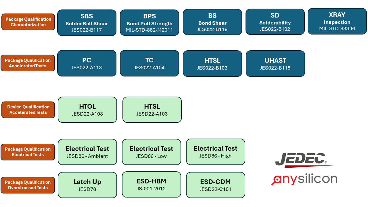
In addition, the following is a typical list of tests conducted to package qualification and reliability testing.
Some qualification tests are related to verifying the ASIC design functionality, the very common tests are:
Some qualification tests are related to quality and reliability tests. Some of the common stress tests are:
JEDEC has a few documents describing the different tests. Below please find our brief description of each test.

ESD test is exposing ICs’ IO pins to transient high voltage to ensure ESD protection. In the ESD semiconductor qualification tests a few test are performed:
HBM ESD (Human Body Model): 2KV
This HBM EDS models the discharge of electricity into a pin through contact with a human body that has been charged with static electricity. 3 units per voltage level are required for HBM testing. Read more about understanding ESD HBM in IC Design.
ESD CDM (Charge Device Model): 0.5KV
CDM ESD testing a model is based on breakdown level on automatic assembly lines. 3 units per voltage level are required for CDM testing. Please read more here: Understanding ESD CDM in IC Design.
MM ESD (Machine Model): 0.2KV
Machine model ESD goal’s to simulate a machine discharging through a semiconductor device to ground. Usually, the stress level of MM ESD is 10 times lower than that of HBM ESD. Typically, the protection voltage level for HBM typically is 2 kV and for MM it is ~200 V.
The latch up testing is a series of attempts that trigger the SCR structure within the CMOS IC while the relevant pins are monitored for over current behavior. 6 units are required for latchup testing. Read more here: What is Latch-Up and how to test it?
High temperature stress testing of ICs while they are biased, typically running for 1000 hours. HTOL test is used to determine device resistance to continued operating stress, both electrical and thermal. 77 units are required per lot, typically 3 inconsecutive lots are needed. JEDEC Spec: JESD22-A108. Read more here: Introduction to HTOL.
High Temperature Storage Life test is performed to stimulate storage conditions. The HTSL testing is done in 125C-150C, without any bias. 25 devices are reuqired per lot. Spec: JESD22-A103. Read more here understanding HTSL
Highly accelerated temperature and humidity stress test, the test is done in 85% and 85C. Specs : JESD22-A110 (biased), JESD22-A118 (unbiased). HAST test definition is Highly Accelerated Stress Test. And requires 25 units per lot. Please read more her: understanding HAST
Preconditioning test is exposing ICs to thermal conditions to simulate the conditions IC will have during PCB soldering process.
Temperature cycling is accelerating ICs failure rate to expose wire bond, bumping, crack issues etc. Spec: JESD22-A104.
If you cannot conduct the qualification tests internally then it’s better to let one vendor manage the entire qualification services tests for you. Get a quote for your ASIC qualification here. Remember that the ICs should be tested before and after the qualification tests, therefore, the IC qualification test vendor should be somewhat close to your test partner. AnySilicon platform consists of top IC qualification vendors, please click here to choose a vendor.
