

This article focuses on the various stages of SoC development. In a typical SoC development, there are many steps that are highly dependent and linked to each other. SoC design flow works on multiple optimization goals and constraints and therefore requires various SoC development skills and EDA tools.
SoC refers to the term System on a Chip. It is a single chip which integrates a whole electronic or a system into it. A SoC may contain digital, analog, mixed-signal devices on the same chip. In a traditional computer system architecture, each system component such as CPU, controller chips, a GPU, and RAM etc., used to be separately installed on the board, but thanks to technological advancements in the semiconductor industry has enabled more and more elements to be integrated in a single silicon chip. A current-day system on a chip (SoC) consists of several different components of a system such as the CPU (a microprocessor or microcontroller), memory, input/output (I/O) interface and wireless blocks, on a single silicon substrate. Most SoCs also use various pre-designed hardware block, called as IP cores, to improve design time to market.
Since it has all the system components on one single chip, SoCs offer the advantages of reduced size, overall system cost, lower power consumption and Increased performance. SoCs are becoming increasingly popular with the growth of mobile computing and IoT (Internet of Things) devices.
Read more about What is a System on Chip (SoC).
Architecture Design This stage involves defining the overall architecture of the SoC, including the selection of functional blocks and their interconnectivity. The goal is to design an SoC system that meets the desired specifications and requirements.
SoC Block Design
It involves designing individual functional blocks that make up the “glue logic” of the SoC the the company propriety technology. These blocks can include processors, hardware controllers, interfaces, peripherals, and other custom blocks. Hardware description languages are often employed to define the behavior and connectivity of these blocks.
Hardware Block and IP Integration
Once the individual hardware blocks are ready, the next step is to integrate them together. This process ensures that the blocks can communicate effectively and function as a cohesive unit.
Verification
Validation and testing play a crucial role in SoC design. At various levels, functional verification is conducted to ensure that the SoC performs as intended. Techniques such as simulation, emulation, and formal verification are employed to validate the correctness and functionality of the design.
Physical Design and Tapeout
Once the design is verified, attention shifts to the physical implementation of the SoC. This involves layout and placement of the design on the actual silicon. The design is optimized for factors such as timing, power, and manufacturing constraints. Finally, the tapeout process refers to the generation of the final design files that are sent for fabrication.
This section explores the different approaches, considerations, compromises, and trade-offs that commonly arise in SoC architecture design.
Approaches: When designing an SoC, there are various approaches to consider. One popular approach is to systematically architect the hardware elements and blocks within the SoC to fulfill dedicated functions. Each hardware component IP core is designed and verified to ensure it behaves as intended. Considerations: In SoC architecture, several considerations must be taken into account. Memory elements, such as flash memory, RAM, and ROM, are carefully selected and integrated within the SoC to meet performance and storage requirements. The choice of specialized processors, such as application-specific instruction set processors (ASIPs) and Digital Signal Processors (DSPs), depends on the specific computational needs of the system.
Power management of SoC is also an important topic in SoC architecture, so circuits are also incorporated to optimize energy efficiency, Techniques such as clock gating, power gating, and voltage scaling are employed to minimize power usage without compromising performance.
Additionally, factors like system reliability, cost, and time-to-market are important considerations throughout the design process.
Compromises and Trade-offs: During SoC architecture design, compromises and trade-offs inevitably arise. For example, designers often need to strike a balance between optimizing performance and managing power consumption. Increasing processing power and adding functionality may lead to higher power consumption, while reducing power usage could limit performance. In addition, optimizing for a smaller form factor may require trade-offs in terms of the number and size of the interconnects and peripherals that can be integrated. Trade-offs regarding cost, complexity, and reliability also need to be carefully evaluated to meet the desired system specifications. Recently, Reprogrammable hardware components (such as eFPGA) are used to ensure an adaptable design, independent of time scales, facilitating updates post-deployment.
SoC development process can be broken into multiple stages as illustrated in the following figure. SoC (System on Chip) design methodology is a multifaceted discipline requiring a comprehensive understanding of both hardware and software aspects. The design flow follows a hierarchical process, beginning with defining and modeling the chip’s design life cycle. It starts with system-level planning and traverses through design, verification, and physical realization.
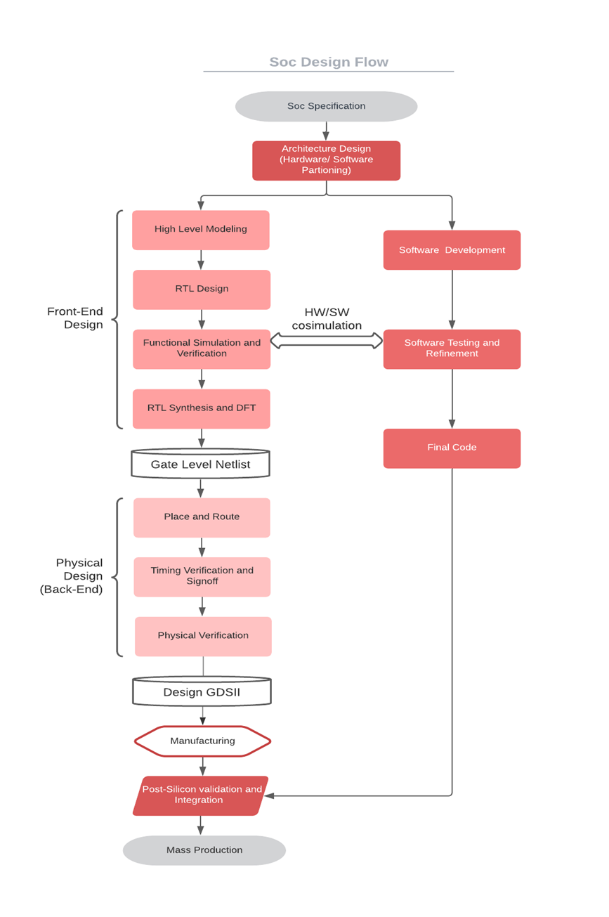
For any SoC development, the first step is to specify the requirements. The specifications are required for both the hardware as well as the software portions of the design. The specifications must completely describe all the interfaces between the design and its environment. To meet the user requirements regarding design of chip, changes are done accordingly in design tools, procedures and software/hardware abilities.
The Hardware Specifications includes the functionality, various hardware components (processors, memories etc), external interfaces to other hardware (pins, buses etc), internal interfaces between hardware components, interface to Software, timing, performance and other physical design details such as area and power.
General Software Specifications includes the functionality, software structure, interface to hardware components, timing and performance of the design.
After gathering all the SoC specifications comes the architecture design. Architecture design consists of behavioral and functional modeling of the specifications. The architecture is specified in terms of combinational logic blocks, data registers, buses, on-chip and off-chip memories, switches, and finite state machines. The optimal architecture development in terms of appropriate balance between cost, power, area, and performance involves a number of complex decisions and tradeoffs, such as deciding which software and hardware components, processor(s), bus architecture and memory architecture to be used.
In this stage the design is partitioned into the hardware and software components. Both the hardware and software components are parallelly developed, tested and refined in the further stages of the design flow.
As the modern day SoC design complexity increases, we can no longer afford to wait for hardware development in order to start developing software. So, both the hardware as well as the software for the SoC is developed and tested concurrently in the design process. Early software development offers its own advantages. The first is verifying the integration of hardware/software interfaces. Often the integration of software with the hardware platform turns up bugs in the software and in the hardware design. Fast, abstract models of the hardware design have enough detail to emulate the hardware and they can run at speeds required for software development and debugging. Fixing the hardware bugs is costly and verifying the hardware/software interface early on can help avoid that. The other advantage is to save the time to market the product. Abstract hardware models can be used in early development of low-level software, e.g. device drivers and firmware. The low-level models can be used for developing higher levels of the application software stack such as middleware and the operating system. Then the developed software can be easily integrated with the hardware within a few weeks of hardware availability.
After the design is partitioned into hardware and software, the hardware components go through various stages of development. At each of these stages the hardware is optimized based on a number of design constraints. Furthermore, the design is simulated, tested, analyzed and refined after each stage to ensure that it is meeting the design requirements. These development stages are discussed further in more detail.
High level modeling is the abstract algorithmic description of various hardware components. This modeling is generally done in C, systemC or other high level languages. At this stage there are no significant concerns about design constraints. It is useful and efficient for generating a compact execution model as the initial design draft.
High-level models of the designs are generally technology independent which allow the possibility of design reuse. High level Synthesis tools convert the high-level design to RTL using various algorithms to optimize the design.
The term RTL refers to Register Transfer Level. This level of design abstraction lies between behavioral description of the desired circuit and a structural one. The RTL describes the circuit as a set of registers and a set of transfer functions describing the flow of data between the registers. But it doesn’t describe the hardware components (such as gates) used to perform these operations. The registers are later implemented using flip-flops and the transfer functions are implemented as blocks of combinational logic. The commonly used languages for RTL development are Verilog and VHDL.
The RTL code is given as input to a logic synthesis tool which generates the gate-level abstraction of the design that is used for all downstream implementation steps.
The developed RTL code needs to be verified for functional correctness before moving to further stages of design. All the bugs found in the verification stage are reported back and the code is refined to fix the issues. This step makes sure that the RTL code is logically correct and matches the behavioral model of the design. During verification, various techniques and numerous suites of tests are developed to check that the design behavior corresponds to the initial specification, followed by simulation to verify the sequential logic.
RTL verification in the early stages of the design helps to identify any bugs or timing issues and ensures that high quality RTL is used for synthesis and place-and-route steps.
Read here about ASIC verification.
Logic synthesis is the process which transforms RTL (verilog or VHDL) code into a gate level netlist that describes the hardware (logic gates and the wires connectivity). Synthesis process involves three steps which are translation, mapping and optimization. With the help of these three steps, it converts RTL code into gate level netlist. The RTL elements are mapped into logic gates using standard cell libraries. These libraries consist of various basic logic gates like AND, OR, NOR, and complex cells like adder, multiplexers, memory, and flip-flops etc. The conversion from RTL code into design with logic gates is generally done with the help of synthesis tools. The popular synthesis tools available are Design Compiler by Synopsys and Genus Synthesis Solution by Cadence. RTL code, technology library and design constraints (clock, IO constraints, power constraints etc) are given as input to the synthesis tool. The synthesis tools map the design elements to target technology libraries and perform various optimizations on the design to achieve better power, performance, timing, and area.
At this stage, often additional test logic is inserted to support design for testability (DFT) features and capabilities in the device. The DFT logic can be used after fabrication to test and debug any faults in the design. This test logic can be inserted in the design at the RTL as well as netlist level based on the design flow. After this, formal verification and simulations are performed on the synthesized gate-level netlist to ensure that there are no problems in the design.
The synthesized gate level netlist is then used for further stages of the physical design process.
Physical Design is the process of translating the gate level netlist into a physical layout. This physical layout consists of various metal shapes and sizes which can be drawn onto masks and manufactured on the silicon wafer.
The Physical Design process can be broken down into multiple stages as illustrated below. It is often an iterative process where a number of optimizations are performed at each step to meet the design performance, area & power requirements.
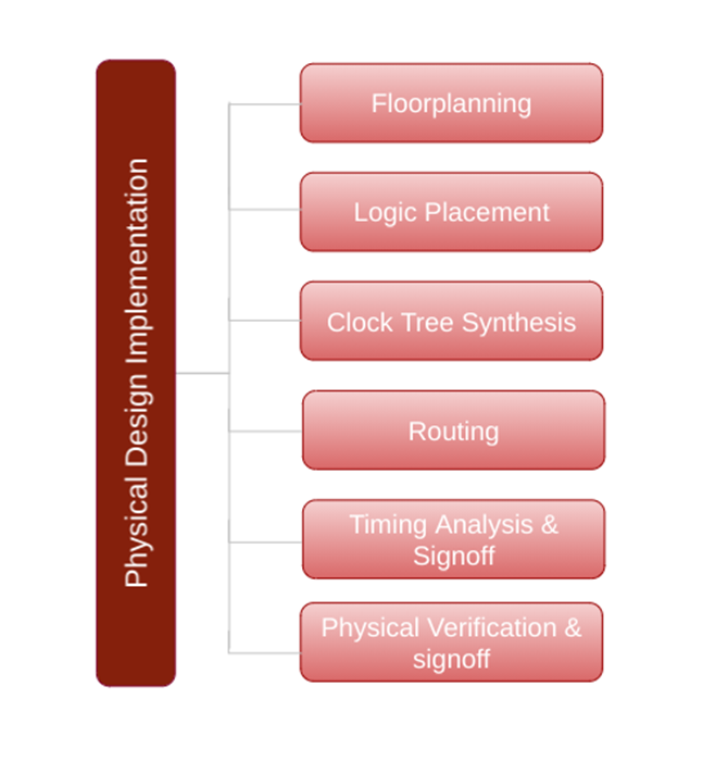
Floorplanning is the first step of physical design. The design is first partitioned into various smaller subsystems based on the system architecture and design requirements. Floorplanning determines the aspect ratio and area of the layout. Here we create the placement rows for standard cells and fix the placement of I/Os around the boundary. Any macros in the design are also placed during the floorplan stage.
Power planning is also typically done during floorplanning. The power grid network is created to distribute power to all the std cells rows, macros and all other components of the design. If there are any special IPs being used in the design then all the IP integration guidelines are also considered in floorplanning.
A good floorplan is very critical to the overall quality of your design.
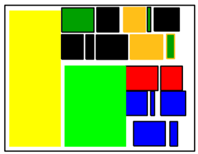
Image Courtesy: Andrew Kahng, UCSD
In this stage all the standard cells in the design are placed and assigned a legal location. After the placement EDA tools performs a number of optimizations to improve placement and congestion. A bad placement might lead to larger area utilization and timing issues.
EDA tools also use timing driven placement algorithms to optimize the placement while considering the timing requirements of the design.
During the Floorplanning & placement stage, the clock is considered as an ideal network. The optimizations in the placement stage are performed based on the assumption of an ideal clock reaching to all flops at the same time. In CTS, a clock network is created to distribute the clock to all flops. This clock tree is built using buffers or inverters along the clock paths of design in order to achieve zero/minimum skew based on design requirement. A good quality clock network is very crucial to meet the timing requirements of the design.
Once all the standard cells are legally placed and the clock network is synthesized, all the connecting data nets need to be laid out on the metal layers. This is done during the routing stage. After routing all the nets, a number of optimizations are performed based on the design timing requirements and analysis.
After the design Routing, static timing analysis is performed on the design. This step is critical to analyze the performance of the design. During STA, we break down the design into timing paths and calculate the signal propagation delay along each path. Then each path is checked for violations of timing constraints. If any path is violated then these violations need to be addressed before signing off on the design.
The timing signoff ensures that all the design elements are meeting the specified timing requirements and the design is working at the desired frequency.
After the routing is completed, the layout must be completely verified to ensure its correct electrical and logical functionality. The physical verification signoff ensures that the design meets all the fabrication specified rules and can be easily manufactured. Various checks that are performed at this stage includes :
DRC (Design Rule Check)
LVS (Layout Vs Schematic)
ERC (Electrical Rule Check)
Antenna check
EM (Electromigration Analysis)
Once the physical verification is done, the layout is streamed out in the form of a gdsII or OASIS file for fabrication which is called design tapeout.
Get a fast indicative cost range, then unlock a full breakdown by email.
At the end of the physical design process, the design is analyzed with STA, simulation and other tools to make sure that it meets the specified operational parameters such as frequency, power consumption, functional integrity and electrical integrity. When all physical design checks are done and the known bugs have been rectified and re-verified, the design gdsII file is sent to the specialized semiconductor fabrication plants, also called foundries or fabs. The gdsII file contains info about each layer of the chip. The foundry uses this information to create the SoC chip.
The manufacturing process largely consists of two steps. The first step, wafer fabrication, is a multi-step sequence of photolithographic and chemical processing steps (such as Photomasking, ionic implantation, metal deposition, diffusion and etching). The wafer is typically made of pure semiconducting material. These steps are repeated several times at different stages of the process. Every step adds a new layer to the wafer or modifies the existing one which gradually forms the electronic circuits. Wafer fabrication often takes place in a highly controlled and extremely clean environment. After the fabrication the silicon chips (also referred as die) are subjected to a number of electrical tests to determine if they function properly.
The second step, assembly, is the precise and automated process of packaging the fully functional silicon chips. The chips are placed on a lead frame and then mounted in a ceramic or plastic package. The package protects the die from external environments and also makes the whole device easier to handle. These packages are available in a range of shapes and sizes depending on the die itself and the application in which it will be used. The packaged chips are again tested to ensure that they were not damaged during the packaging process.
Read more about static timing analysis.
The goal of post-silicon validation is to make sure that the SoC device works properly in the actual working environment while executing real design software. Since a modern SoC design is an integration of various hardware (multiple processors, IPs, memories and on-chip communication network) and software components, the post-silicon validation is a complex co-validation process across hardware, software, and peripheral functionality. Hardware and Software compatibility validation is necessary to ensure that the silicon chip works with different versions of systems and application software. These Validation checks can also include many different things such as functional correctness, compliance to power and performance constraints for target use-cases, electrical noise margins tolerance, robustness against physical stress or thermal changes in the environment, and so on.
Post-Silicon validation is quite different from the pre-silicon, where the validation target is usually a computerized model of the design rather than an actual silicon die. The post-silicon validation offers the benefit of running at real system speeds ( range of GHz), as the tests are performed on the manufactured silicon chips. So, this is quite faster than the pre-silicon verification. But on the other hand, post-silicon validation is more complex due to the physical nature of the validation target. it is much more difficult to observe, control and debug an actual silicon device rather than a computerized model. In addition, post-silicon validation is usually done on a strict schedule, in order to meet the time-to-market requirements.
The finished SoC devices can be used in a variety of products such as personal computers, mobile phones and cars in everyday life.
EDA tools are very crucial to SoC design as they help in designing very complex integrated circuits. The use of EDA tools helps reduce time in designing, testing & reducing production costs.
Some of the popular tools used in various stages of SOC development flow are the following :
RTL tools :
Logic Synthesis tools :
Place and Route tools :
Static timing analysis tools :
Physical Verification tools :
Formal Verification tools :
DFT tools :
Gate level Simulation tools :
Power analysis tools :
