

Application-Specific Integrated Circuits (ASICs) and SoCs play a critical role in modern technological advancements. These customized integrated circuits are designed to cater to specific applications, offering optimized performance, power efficiency, and cost-effectiveness. Understanding the economics behind ASICs is essential for businesses and industries that rely on these chips. This article explores the economics of ASICs, focusing on the cost of design and development, cost of manufacture, testing, packaging, and their diverse applications.
Get a price of ASIC fabrication from vetted suppliers – ASIC Design Service.
The cost of design and development of an ASIC (Application-Specific Integrated Circuit) encompasses various components that contribute to the overall expenses. Let’s explore these components in detail:
ASIC design requires a team of highly skilled engineers with expertise in digital and analog circuit design, verification, and physical implementation. The cost of employing these professionals or engaging specialized design firms is a significant component of the overall expense. The expertise, experience and the geographical location of the design teams influence the complexity and efficiency of the ASIC design process.
The engineering expertise needed for designing a chip has evolved over the decades. The last decade saw a growing need for automation, thereby needing more software expertise to design chips. This decade, however, there has been a surge in using artificial intelligence/machine learning to improve the overall design efficiency and therefore attracting engineering with appropriate skills.
Sophisticated Electronic Design Automation (EDA) tools are essential for ASIC design as they streamline the ASIC design flow, enable efficient exploration of design trade-offs, enhance productivity and improve chances of a successful ASIC development. These tools enable engineers to:
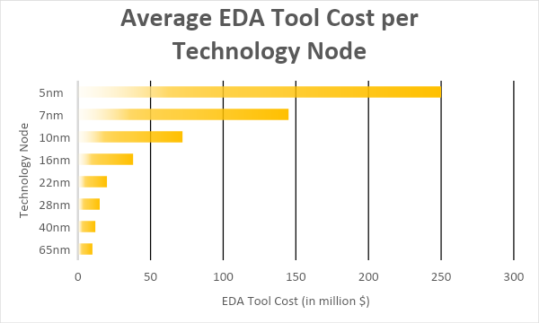
The cost of licensing EDA tools can be substantial, especially for advanced and feature-rich software suites. The complexity of the ASIC design and the required functionality often dictate the selection and cost of the design tools.
ASIC development can be expedited by incorporating pre-designed circuits or modules known as Intellectual Property (IP). Acquiring third-party IP licenses allows designers to leverage existing proven designs and reduce development time. However, these licenses come at a cost, and the complexity and uniqueness of the required IP affect the overall development expenses.
Intellectual property licensing is key to avoid any infringement cases where the rights holders of any technology whether that be in the form of patents, trademarks, trade secrets or copyrights can pursue legal action to seek damages and injunctions to prevent further infringement.
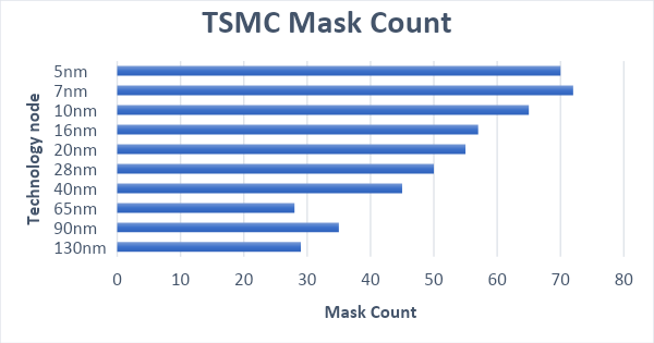
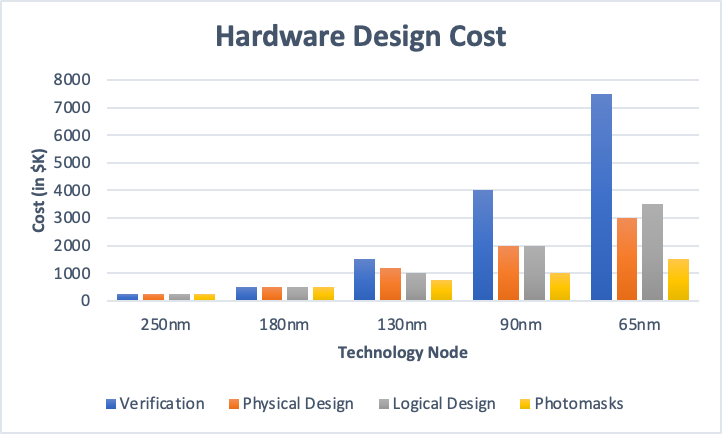
Once the ASIC design is complete, a set of masks is required for ASIC fabrication. These masks define the circuit layout and are used during the manufacturing process. The cost of creating mask sets is influenced by factors such as the complexity of the design, the number of layers in the layout, and the manufacturing process technology. Additionally, prototypes are often fabricated to validate the design before mass production, contributing to the overall cost of development.
ASIC designs undergo rigorous verification and testing to ensure functionality, performance, and reliability. Verification involves simulating and analysing the design under various scenarios to identify and fix any design flaws or errors. The cost of verification includes the time and resources spent on simulation tools, test benches, and verification engineers. Furthermore, comprehensive testing is conducted on fabricated ASICs to validate their functionality, adding to the overall development cost.
ASIC development often involves multiple iterations and engineering changes to optimize the design and address any issues discovered during testing. Iterations may require additional engineering time, prototyping, and testing, resulting in increased costs. Efficient project management and design methodologies can help minimize the number of iterations and associated expenses.
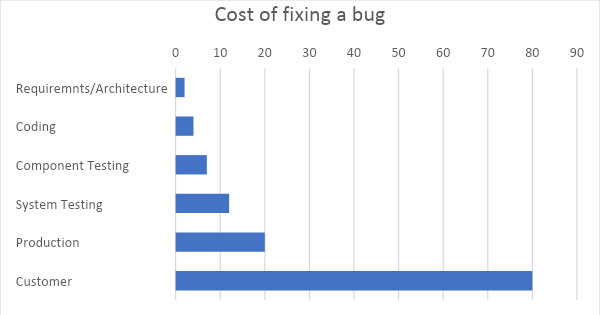
The cost of fixing a bug increases exponentially depending on the time it is found and corrected. It is catastrophic to find a bug during the production and even worse if found when the manufactured devices have been shipped to the customer.
The development of ASICs requires comprehensive documentation, including design specifications, datasheets, application notes, and compliance documentation. Generating and maintaining these documents incurs costs, especially in industries with stringent regulatory requirements.
The time required to develop an ASIC affects the cost. Faster development cycles may involve higher expenses due to the need for additional resources, dedicated engineering teams, or prioritized design services. The cost of delayed market entry or missed opportunities should also be considered when evaluating the economics of ASIC development.
Understanding and managing these components of the cost of design and development is crucial for ASIC projects. Careful planning, efficient resource allocation, and effective project management techniques can help optimize costs while ensuring the successful development of ASICs tailored to specific applications.
Once the ASIC design is complete, the manufacturing process begins. ASIC fabrication involves several cost factors:
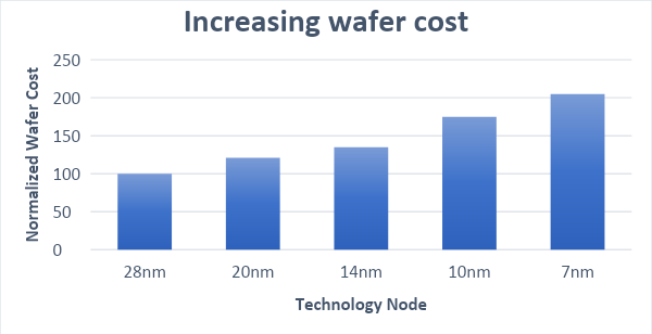
a) Wafer Fabrication: The ASIC design is etched onto a silicon wafer during the fabrication process. Foundries, specialized manufacturing facilities, handle the fabrication. The cost is determined by the size of the wafer, the number of chips per wafer, and the manufacturing process technology (e.g., 7nm, 10nm, etc.). The smaller the process node, the higher the manufacturing cost.
b) Yield and Defects: During fabrication, defects can occur that render certain chips non-functional. The yield, which represents the percentage of functional chips per wafer, impacts the overall manufacturing cost. Lower yields increase the cost per functional chip because it requires additional time and resources to identify and discard the defective chips. Higher yield enables more efficient use of time and resources, thereby reducing the overall manufacturing cost.
c) Foundry Selection: Different foundries offer varying levels of technology, quality, and cost. Choosing a foundry involves evaluating these factors to optimize cost and production efficiency.
After fabrication, ASIC chips go through testing and packaging stages before they are ready for deployment:
a) Testing: Each ASIC chip is tested to ensure its functionality, performance, reliability and quality standards. Test equipment and resources, along with the time spent on testing, contribute to the overall cost. Complex ASICs may require specialized test equipment, adding to the testing expenses. Factors that affect the test cost are:
In average, the packaging tooling of a wafer sort solution that includes both hardware and software is approximately USD 75K, and for a final test solution that includes both hardware, software and socket is USD 100K. Please use our form to receive price offers directly from testing vendors.
b) Packaging: Once tested, ASIC chips are packaged to protect them from environmental factors and facilitate integration with larger systems. Packaging costs include materials, assembly, and testing of the packaged chips. Examples of packages include Ball Grid Arrays (BGAs), Flip-Chip BGA (FCBGA), Ceramic Dual In-line Package (Ceramic DIP) etc.
In average, the packaging tooling of QFN with a new lead frame is approximately USD 15K, and for a wire-boned BGA with a new substrate is USD 45K. Please use our form to receive price offers directly from packaging vendors.
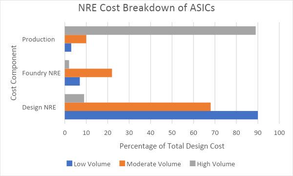
The volume of ASIC production directly affects the cost per unit. Generally, higher volumes result in economies of scale, leading to reduced per-unit manufacturing costs. However, initial low-volume production can incur higher costs due to limited production yield, higher NRE costs per unit, and setup costs. As production volumes increase, cost optimization becomes possible through negotiation with suppliers, better yield management, and improved production efficiency.
The graph below highlights the cost breakdown of ASICs depending on the volume of chips manufactured. As the volume increases, the design NRE and the foundry NRE costs become a small fraction of the overall production costs, while for low volume, the production costs are dominated by the design NRE costs.
ASICs find applications across various industries, offering numerous benefits such as enhanced performance, power efficiency, and cost optimization:
The economics of ASICs involve multiple cost factors, including design and development, manufacturing, testing, and packaging. The investment in engineering expertise, design tools, IP licensing, mask sets, and prototypes significantly contribute to the design and development cost. Manufacturing costs are determined by wafer fabrication, yield, defects, and foundry selection. Testing and packaging costs ensure the functionality and integration of ASIC chips into larger systems. Despite the initial expenses, ASICs offer substantial advantages in various industries, enabling high-performance, cost-effective solutions tailored to specific applications. Understanding the economics of ASICs is crucial for businesses and industries to make informed decisions and capitalize on the benefits offered by these specialized integrated circuits.
References:


