The strongest takeaway from TSMC’s 2026 North America Technology Symposium is that the old model of simple node-to-node progression is fading. In its place, TSMC is building a roadmap that separates cost-efficient scaling from performance infrastructure, with some technologies aimed at smooth migration and others designed to solve the physical constraints of AI and HPC.
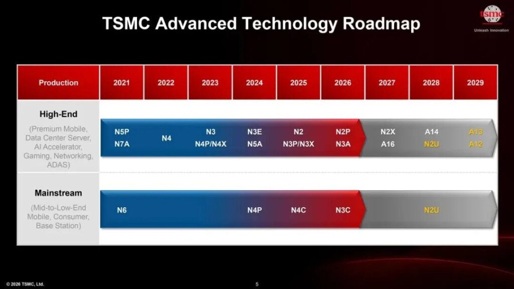
That shift matters. For years, semiconductor roadmaps were often interpreted as a straightforward march from one geometry to the next: 7nm to 5nm, then 3nm, then 2nm, and beyond. But at the leading edge, that logic is no longer sufficient. The technical and economic demands of different chip categories are diverging too sharply. A smartphone SoC does not face the same design priorities as a large AI accelerator. A mobile processor may prioritize die size, power efficiency, and fast reuse of validated IP. An AI or HPC device, by contrast, is increasingly constrained by power delivery, routing congestion, current density, thermal behavior, and packaging scale. TSMC’s latest roadmap reflects that divide clearly.
The newly highlighted technologies — including A13, A12, and N2U — suggest that TSMC is no longer treating leading-edge logic as a single ladder. It is now better understood as a branching platform strategy. Some branches are intended to maximize continuity and economic efficiency. Others are meant to address the deeper structural bottlenecks of advanced compute.
A13 is one of the clearest examples of the first category. On the surface, it may not look like the most dramatic announcement in the roadmap. It is not being positioned as a disruptive reset or a radical break in design philosophy. Instead, its importance comes from how deliberately it reduces friction. TSMC has framed A13 as a direct shrink of A14 with backward-compatible design rules, allowing customers to migrate more efficiently. That point is more significant than it may first appear.
At advanced nodes, process migration is not simply a matter of buying more expensive wafers. Every node transition has implications across IP reuse, standard cell migration, analog redesign, EDA flow qualification, verification effort, signoff closure, timing re-optimization, and reliability validation. Those costs add up quickly. In that environment, a node that minimizes migration burden can be commercially more powerful than one that introduces a more dramatic technical leap but forces a larger reset across the design stack.
That is why A13 matters. Its value is not only in its density or area benefit, but in its role as a lower-friction extension of an already established platform. For customers building high-volume mobile or client devices, that kind of continuity is strategically attractive. It enables them to preserve prior design investment, shorten development cycles, reduce porting effort, and improve economic returns without abandoning the benefits of scaling. In that sense, A13 represents a broader principle that is becoming more important across the semiconductor industry: scaling is no longer just about achieving the next transistor milestone, but about extracting more value from the ecosystem surrounding a process node.
This makes A13 especially relevant for mobile and client markets, where cost discipline and platform reuse remain central. These segments often benefit more from predictable migration and strong design continuity than from a disruptive process shift that requires extensive redesign. The semiconductor industry has long celebrated breakthrough nodes, but increasingly, the more valuable offering may be the one that extends prior work with the least disruption. TSMC appears to understand that clearly.
N2U fits into a similar pattern, though with a slightly different emphasis. Its importance lies in how it extends the life and usefulness of the 2nm family. Rather than presenting N2 as a one-time node introduction followed immediately by a separate new platform, TSMC is building a broader N2 ecosystem with variants that serve different needs over time. N2U reinforces the idea that the value of a node family is not limited to the first version that reaches production. Instead, the family becomes a foundation for multiple product cycles, derivative designs, and performance optimizations.
That kind of strategy matters because semiconductor development rarely happens in a single isolated product generation. Companies often build one major chip, then expand into follow-on versions, cost-optimized variants, and more specialized derivatives. A platform such as N2U allows them to keep benefiting from the ecosystem around the original node while still capturing incremental improvements in power, speed, and density. It also lowers the risk of premature migration to a more disruptive process generation when a refined platform may be sufficient.
The larger point is that TSMC is increasingly competing not only on transistor technology, but on platform continuity. That includes IP compatibility, PDK stability, design reuse, EDA alignment, and migration economics. In earlier years, foundry leadership was often discussed primarily in terms of who reached the smallest feature size first. Today, the more meaningful question may be which company gives customers the best balance of performance, manufacturability, ecosystem maturity, and return on design investment. N2U fits squarely into that model.
If A13 and N2U represent continuity and platform leverage, A16 and A12 represent a different kind of response entirely. These technologies are better understood as infrastructure-oriented solutions for the emerging constraints of AI and HPC.
That distinction is important. In the AI era, raw transistor scaling is no longer the only or even always the primary limiter. Large accelerators increasingly run into problems of power distribution, routing congestion, thermal density, interconnect overhead, and package-level complexity. Delivering more current across large, dense die areas while maintaining signal integrity and performance headroom is becoming a major challenge. Traditional frontside routing forces power and signal paths to compete for routing resources, which can create inefficiencies as transistor density rises.
This is where backside power delivery becomes strategically important. TSMC’s Super Power Rail approach, associated with A12 and already reflected in the direction of A16, is meant to address that problem by moving power delivery to the backside of the wafer. Conceptually, this allows frontside interconnect resources to be used more efficiently for signaling while improving power distribution across the die. The benefit is not simply “better scaling” in the conventional sense. It is a structural improvement to how advanced logic handles one of its most difficult constraints.
That is especially relevant for AI and HPC devices, where the practical problem is not just how many transistors can fit on a chip, but how effectively those transistors can be powered, cooled, and connected at system scale. In that environment, the process node becomes part of a much larger performance architecture. A12 and A16 reflect that shift. They are not just smaller nodes. They are technologies aimed at enabling the continued growth of large compute engines under increasingly difficult electrical and thermal conditions.
It is also worth noting that backside power delivery is not a universal answer for every product. It brings added complexity in process integration, design methodology, and ecosystem support. That is one reason TSMC’s broader roadmap remains diversified. Not every customer will want to move immediately to that model, and not every design needs it. Some customers may prefer a path that preserves more conventional integration while still delivering strong frequency or performance characteristics.
That is where technologies like N2X remain relevant. A high-performance branch of the N2 family can serve customers who want leading-edge performance but may not yet be ready to adopt a more disruptive power-delivery architecture. This reinforces the broader message of the roadmap: advanced logic is no longer one path for all customers. It is a set of differentiated options designed around distinct technical and commercial priorities.
One of the most striking signals in the roadmap is not only what TSMC is introducing, but also what it is choosing not to adopt in the near term. The company’s decision not to rely on High-NA EUV through this roadmap window is highly revealing. In some corners of the industry, High-NA EUV is treated as the obvious next step in lithography progression. But TSMC appears to be taking a more disciplined view.
That choice reflects a practical manufacturing philosophy. High-NA EUV promises technical advantages, but it also comes with major capital cost, tooling complexity, mask implications, ecosystem demands, and uncertain near-term economic benefit. If current EUV infrastructure can still support competitive scaling with acceptable yield and cost, then early migration to a more expensive lithography regime is not necessarily a commercial advantage. In semiconductor manufacturing, being first to adopt a new tool is not always the same as being best positioned to ramp it efficiently at scale.
This is consistent with one of TSMC’s long-standing strengths: process innovation guided by manufacturing judgment. The company’s leadership has never been based purely on technical ambition in isolation. It has also been based on knowing when to push aggressively and when to extend a mature approach for better economics, stronger yields, and broader customer benefit. That mindset appears to be fully intact in the 2026 roadmap.
The result is a strategy that feels more mature and more selective than the simple node races of the past. Instead of chasing the appearance of leadership through the most aggressive possible adoption of every new manufacturing technology, TSMC is aligning its roadmap around differentiated customer needs. A13 supports economically efficient scaling and low-friction migration. N2U extends the practical value of a major platform. A16 and A12 address the deeper power-delivery and integration problems of the AI era. And the continued use of existing EUV reflects a willingness to prioritize manufacturability and ROI over symbolism.
Taken together, these decisions point to a broader industry reality. The next phase of semiconductor competition will not be decided by transistor density alone. It will be shaped by how well foundries manage the interaction between process technology, power architecture, packaging, design ecosystems, and manufacturing economics. The leading edge is becoming more system-oriented, more application-specific, and more dependent on platform strategy.