



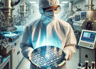
May 26th, 2026 — ASML expects the first semiconductor products manufactured using its next-generation High-NA EUV lithography machines to arrive within months, marking an important milestone for advanced chip manufacturing. The update comes at a time when the semiconductor industry is debating not whether High-NA EUV will be needed, but when it becomes economically justified for high-volume production.
According to Reuters, ASML CEO Christophe Fouquet said the first chips produced with High-NA EUV machines are expected within a few months. The same report noted that the machines can cost up to approximately $400 million each, which has made some customers cautious about early adoption. TSMC, currently the world’s largest pure-play foundry, has reportedly decided that High-NA EUV remains too expensive for now, while Intel, Samsung and SK hynix are moving ahead with adoption plans.
TrendForce also reported that ASML expects early High-NA EUV products in both memory and logic applications, even as TSMC takes a more cost-driven approach and delays the technology for its near-term roadmap.
For the semiconductor industry, this is a significant moment. High-NA EUV has been discussed for years as the next major step in lithography. Now, the technology is beginning to move from R&D and early process development into real product manufacturing.
High-NA EUV is the next generation of extreme ultraviolet lithography. Standard EUV systems use a numerical aperture of 0.33, while ASML’s High-NA EUV systems use a numerical aperture of 0.55. In simple terms, a higher numerical aperture improves the tool’s ability to focus light and print smaller features on silicon wafers.
ASML says its EXE High-NA EUV systems use 13.5 nm EUV light and 0.55 NA optics to provide higher contrast and a resolution of around 8 nm. The company has also stated that High-NA EUV can print transistors around 1.7 times smaller and support transistor densities up to 2.9 times higher compared with previous-generation NXE EUV systems.
This matters because advanced logic and memory chips require extremely fine patterning. As transistor dimensions shrink, chipmakers must either use more advanced lithography or rely on complex multi-patterning techniques. Multi-patterning can increase process complexity, cycle time, cost and defect risk. High-NA EUV is intended to reduce some of that complexity by printing finer features with fewer exposure steps.
ASML is the only company in the world that supplies EUV lithography machines. This gives it a central role in the future of advanced semiconductor manufacturing. If High-NA EUV begins producing real logic and memory chips, it would confirm that the technology is moving beyond pilot-line validation.
The first High-NA EUV chips will likely not mean immediate broad adoption across the industry. Early products may be test chips, limited-volume devices, or specific layers within advanced logic and memory processes. However, even limited early production is important because it helps validate the tool, the process flow, the masks, the resists, the metrology and the broader manufacturing ecosystem.
High-NA EUV adoption is not just about buying a new scanner. It affects almost every part of the manufacturing flow, including mask infrastructure, photoresist performance, overlay control, defect inspection, computational lithography and design rules. This is why the first working products are an important milestone.
The most interesting part of the story is not simply that High-NA EUV is progressing. It is that TSMC appears to be taking a more cautious approach.
TSMC has reportedly indicated that High-NA EUV is too expensive for now. Reuters noted that ASML’s High-NA EUV tools may cost up to approximately $400 million per machine, and that TSMC has viewed the cost as difficult to justify at this stage.
This does not mean TSMC is technically behind. In fact, it may reflect TSMC’s strength. TSMC has historically been very disciplined about manufacturing economics. If it can achieve the required performance, density and yield targets using existing low-NA EUV tools and multi-patterning, then delaying High-NA EUV may make sense.
For a foundry, the best technology is not always the most advanced tool available. The best technology is the one that delivers the right balance of performance, yield, cost, cycle time and customer value.
High-NA EUV may reduce patterning complexity in the long term, but the first generation of tools comes with high capital cost, ecosystem changes and learning-curve risk. TSMC may prefer to wait until the technology becomes more mature, more productive and more economically attractive.
While TSMC is cautious, other major chipmakers are moving forward. Intel has been one of the most aggressive early adopters of High-NA EUV. Intel installed the first commercial High-NA EUV system from ASML at its Oregon R&D fab, and the tool is part of Intel’s roadmap for future advanced nodes.
Intel’s interest is easy to understand. The company is trying to regain process leadership and build a competitive foundry business. High-NA EUV gives Intel a potential technology differentiator, especially for its upcoming 14A node and later angstrom-class technologies.
Samsung also has strong motivation to adopt High-NA EUV. As a leading logic and memory manufacturer, Samsung competes directly with TSMC in foundry and with SK hynix and Micron in memory. Early access to High-NA EUV could support future DRAM, logic and advanced packaging strategies.
SK hynix is especially relevant because High-NA EUV may be useful for advanced memory scaling. As AI systems drive demand for high-bandwidth memory, DRAM manufacturers need continued improvements in density, performance and energy efficiency. High-NA EUV could eventually help memory makers reduce patterning complexity in advanced DRAM processes.
High-NA EUV may be adopted differently in logic and memory.
In logic manufacturing, the main drivers are transistor density, performance, power efficiency and routing complexity. Advanced CPUs, GPUs, AI accelerators and networking ASICs all require dense and precise patterning. High-NA EUV could help reduce the number of lithography steps needed for the most critical layers.
In memory manufacturing, the economics are different. Memory is extremely cost-sensitive, and manufacturers must justify every process step against bit-cost reduction. For DRAM, High-NA EUV may become attractive if it enables tighter patterning with fewer process steps or better yield. For NAND, the scaling model is more vertical, so High-NA EUV may be less immediately central than in logic or DRAM.
This is why ASML’s expectation of early High-NA EUV products in both memory and logic is important. It suggests the technology is not limited to one narrow use case.
At first glance, a $400 million lithography machine sounds like it would increase cost. In the short term, that is true. High-NA EUV tools require very large capital investment, and fabs must also invest in supporting infrastructure.
However, ASML argues that High-NA EUV can reduce patterning cost over time. The reason is that one High-NA EUV exposure may replace multiple lower-resolution patterning steps. If a chipmaker can reduce multi-patterning, it may save on masks, process steps, cycle time, overlay risk and yield loss.
The business case therefore depends on the full process flow, not only the scanner price. A very expensive tool can still be economically attractive if it simplifies the manufacturing process enough and if wafer volume is high.
This is the key disagreement in the industry right now. ASML believes High-NA EUV will create long-term value by lowering patterning cost. TSMC appears to believe that, at least for now, the economics do not justify immediate adoption.
For fabless semiconductor companies, High-NA EUV is important but should not be viewed in isolation. A node using High-NA EUV is not automatically better than a node using low-NA EUV. Customers care about final chip performance, power, area, cost, yield, IP availability, design rules and schedule predictability.
High-NA EUV could eventually enable more aggressive design rules and better scaling. But early in the adoption cycle, customers may also face risk from immature process design kits, changing design rules, limited IP availability and yield learning.
This means that for many chip companies, the foundry decision will remain practical. The question is not simply, “Does the node use High-NA EUV?” The better question is: “Can this foundry deliver my chip on time, at the right cost, with acceptable yield and enough ecosystem support?”
AI is one of the biggest forces behind advanced-node demand. Large AI accelerators require enormous transistor counts, high-speed memory interfaces, advanced packaging and strong power efficiency. These chips are expensive to design and manufacture, so even small improvements in density and performance can matter.
At the same time, AI chips are also pushing the limits of semiconductor manufacturing capacity. ASML’s CEO has warned that the chip market could remain supply-constrained as AI, robotics and satellite demand continue to grow.
High-NA EUV may become one of the technologies that helps the industry continue scaling AI processors. However, it will not solve every bottleneck. Advanced packaging, HBM supply, substrate capacity, power delivery and thermal management are also critical.
The decision to adopt High-NA EUV is strategic. A chipmaker must decide not only when to buy the tool, but how to align it with future process nodes, customer demand and capacity planning.
For Intel, early adoption may help support its effort to differentiate Intel Foundry and regain technology leadership. For Samsung and SK hynix, High-NA EUV could support both logic and memory competitiveness. For TSMC, delaying adoption may protect margins and avoid unnecessary early capital expenditure.
None of these strategies is automatically right or wrong. Each company has different priorities. Intel may need a technology leap. TSMC may prefer manufacturing discipline. Memory makers may adopt High-NA EUV only where it improves bit economics.
ASML’s expectation that the first High-NA EUV chips will arrive within months is an important milestone for the semiconductor industry. It shows that High-NA EUV is moving closer to practical production and may soon play a role in both logic and memory manufacturing.
At the same time, TSMC’s cost-driven delay shows that the industry is not adopting the technology uniformly. High-NA EUV offers major technical advantages, but its high cost means chipmakers must carefully evaluate whether it improves the full manufacturing equation.
The next phase of High-NA EUV adoption will be shaped by real production data: yield, throughput, overlay, defectivity, cycle time and cost per wafer. If the technology proves that it can reduce patterning complexity and support better economics, adoption will accelerate. If the cost remains too high, some manufacturers may continue extending low-NA EUV longer than expected.
For semiconductor companies, the key takeaway is clear: High-NA EUV is no longer just a future concept. It is entering the manufacturing roadmap, but its adoption will depend as much on economics as on technical capability.
AnySilicon Connection Service
Choose an option and leave your email. We will connect you with the right person.
Tell us what you're building and we'll recommend qualified vendors for your project.
Free • No obligation • Response within 24 hours