



Developing a custom Power Management Integrated Circuit (PMIC) requires specialized expertise in analog and mixed-signal design, voltage regulation, high-voltage semiconductor devices, power efficiency, and integrated circuit manufacturing.
Whether your application involves automotive electronics, AI data centers, robotics, industrial equipment, medical devices, or battery-powered products, a custom PMIC can help optimize power consumption, reduce PCB size, minimize component count, and improve overall system integration.
AnySilicon connects companies with experienced PMIC and power management ASIC design partners, supporting projects from initial architecture and process selection through circuit design, tapeout, silicon validation, and production.
Tell us about your PMIC requirements and find suitable semiconductor design partners.
A Power Management Integrated Circuit controls, converts, regulates, distributes, or monitors electrical power within an electronic system.
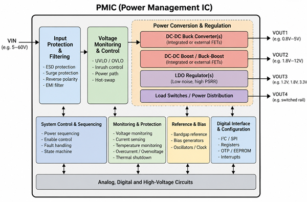
Many modern electronic products require several power supply rails operating at different voltage and current levels. For example, a processor-based system may require 0.8V for a digital core, 1.8V for memory, and 3.3V for peripheral interfaces.
Rather than using multiple independent power management devices, a custom PMIC can integrate several functions into one semiconductor chip.
Typical integrated functions include:
Depending on the application, a PMIC may integrate power transistors or drive external MOSFETs.
The appropriate architecture depends on operating voltage, output power, semiconductor technology, thermal performance, efficiency, and cost requirements.
Custom power management ASICs are used across a wide range of electronic systems.
| Application | Typical PMIC Requirements |
|---|---|
| Automotive electronics | High-voltage operation, diagnostics, sequencing, functional safety |
| AI and data-center systems | High-current power control, monitoring, efficient power conversion |
| Robotics | Motor power control, multiple voltage rails, protection |
| Industrial automation | Wide input voltage, robust protection, reliable operation |
| Battery-powered IoT | Ultra-low standby current, power-path management |
| Medical electronics | Low-noise supply rails, monitoring, high reliability |
| Smart glasses and wearables | Compact design, low quiescent current, battery charging |
| Drones | Lightweight power systems, voltage conversion, fault protection |
| Consumer electronics | Multirail power management, cost and board-space optimization |
For example, a robotics manufacturer may require a custom PMIC integrating several DC-DC controllers, LDOs, voltage monitoring circuits, and protection features.
Similarly, an automotive supplier developing a 48V electronic system may require a high-voltage power management ASIC using a suitable BCD semiconductor process.
A custom PMIC may combine power conversion, analog control, digital logic, and safety functions.
A representative architecture includes:
Power Input → Protection & Monitoring → DC-DC Controllers / Regulators → Multiple Output Rails
Supporting functional blocks may include power sequencing, references, voltage monitors, current sensing, temperature sensors, digital control logic, and nonvolatile configuration memory.
A major design consideration is the integration of high-voltage power circuitry with low-voltage analog and digital logic.
Electrical noise, switching losses, device isolation, thermal management, and electromagnetic compatibility must be addressed throughout the design.
For multirail systems, startup and shutdown sequencing is particularly important to ensure that processors, memories, and peripheral devices receive power in the correct order.
FIND CUSTOM PMIC DESIGN COMPANIES – GET 3 QUOTES
Before approaching an ASIC design company, customers should define their main electrical requirements.
The following example represents a hypothetical industrial power management ASIC.
| Parameter | Example Design Requirement |
|---|---|
| Input voltage | 6V–60V |
| Output voltage rails | 1.2V, 1.8V, 3.3V, 5V |
| DC-DC converter channels | 2–4 |
| LDO channels | 2–6 |
| Switching frequency | 500kHz–3MHz |
| Target converter efficiency | 90–95% at specified load |
| Quiescent current | Application dependent |
| Control interface | I²C / SPI |
| Protection | UVLO, OVP, OCP, thermal shutdown |
| Operating temperature | −40°C to +125°C |
| Potential process | 180nm or 130nm BCD |
| Package | QFN or thermally optimized package |
These are illustrative design targets, not specifications for an existing product. Efficiency depends on converter architecture, external components, load, and operating conditions.
Important technical parameters include output accuracy, transient response, power dissipation, quiescent current, switching noise, and protection response time.
Many power management ICs are developed using BCD (Bipolar-CMOS-DMOS) technologies that support combinations of analog circuits, digital logic, and high-voltage power devices.
The appropriate technology depends on the required voltage, device performance, integration level, and foundry options.
| Semiconductor Technology | Potential Applications |
|---|---|
| 350nm HV / BCD | High-voltage analog and industrial power control |
| 180nm BCD | PMICs, motor-control ICs, gate drivers, industrial applications |
| 130nm BCD | Mixed-signal PMICs, battery-related control, high-voltage integration |
| 110nm BCD-on-SOI | Automotive and industrial smart-power applications |
| 65nm / 55nm BCD | More highly integrated power management with additional digital circuitry |
| Advanced CMOS | Low-voltage digital-intensive power-management functions |
A smaller process geometry is not automatically the most cost-effective option.
For example, a mature 180nm BCD process may offer suitable high-voltage devices, analog components, and manufacturing economics for a particular power-control application.
A more advanced BCD platform may be attractive when additional digital control functionality, integration density, or lower on-resistance is important.
Actual device voltage ratings, isolation options, embedded memory, thick-metal availability, and design rules must be verified for the selected foundry process.
Custom PMIC development involves non-recurring engineering (NRE) expenses, including circuit design, simulation, verification, physical layout, and silicon validation.
The overall cost varies significantly depending on the number of power channels, voltage requirements, process technology, reused IP, qualification requirements, and development scope.
| Project Scope | Indicative Budget (USD) |
|---|---|
| Feasibility study and architecture definition | $30,000–$100,000 |
| Relatively simple custom PMIC | $300,000–$800,000 |
| Multichannel mixed-signal PMIC | $800,000–$2 million |
| Complex high-voltage or automotive PMIC | $2 million+ |
These figures are preliminary planning estimates, not verified market averages or binding quotations. Depending on the project, mask sets, fabrication, packaging, test development, third-party IP, qualification, and additional silicon revisions may incur separate costs.
Multiproject Wafer (MPW) programs can reduce initial fabrication expenses by allowing multiple designs to share mask and wafer manufacturing costs.
As an example, the published EUROPRACTICE 2026 schedule provides the following standard fabrication prices:
| Foundry Process | Published MPW Price |
|---|---|
| GlobalFoundries 130nm BCDlite | €1,760/mm², minimum charged area 12mm² |
| GlobalFoundries 55nm BCDlite | €5,170/mm², minimum charged area 9mm² |
These correspond to minimum listed fabrication charges of approximately €21,120 and €46,530, respectively, before additional costs.
Prices depend on the specific program, eligibility, applicable design rules, and service scope. These published figures are examples of prototype fabrication pricing, not complete PMIC development quotations or guarantees of commercial MPW access.
REQUEST A CUSTOM PMIC DESIGN COST ESTIMATE
A new custom mixed-signal PMIC may require approximately 15–24 months to reach production readiness, depending on technical complexity, qualification requirements, manufacturing schedules, and whether silicon revisions are necessary.
A representative schedule is shown below.
| Development Phase | Indicative Timeline |
|---|---|
| Requirements and feasibility | Months 1–2 |
| Architecture and process selection | Months 2–4 |
| Analog and digital circuit design | Months 4–9 |
| Layout, verification, and signoff | Months 8–12 |
| Tapeout, wafer fabrication, and packaging | Months 12–16 |
| Silicon testing and characterization | Months 16–20 |
| Qualification and production preparation | Months 20–24 |
Several phases overlap. The timeline is illustrative and assumes no major redesign.
Key technical verification activities include circuit simulation, process-voltage-temperature analysis, Monte Carlo simulation, power-integrity analysis, thermal evaluation, and reliability verification.
For automotive and safety-related applications, qualification and functional safety requirements can add further development effort and time.
Using a standard PMIC is normally preferable when an available product meets the system requirements, particularly for lower production volumes or short development schedules.
A custom PMIC becomes more attractive when it can reduce recurring system cost, improve performance, or consolidate several components.
Consider the following hypothetical commercial example:
| Parameter | Example |
|---|---|
| Custom PMIC development NRE | $600,000 |
| Annual production volume | 200,000 units |
| Product lifetime | 4 years |
| Total expected volume | 800,000 units |
| Existing power-management solution cost | $3.80/unit |
| Custom solution recurring cost | $2.60/unit |
| Recurring saving | $1.20/unit |
| Total savings before NRE | $960,000 |
| Net saving after assumed NRE | $360,000 |
Under these assumptions, the break-even point occurs after approximately 500,000 units, or 2.5 years at 200,000 units annually.
The calculation assumes that all relevant recurring costs are reflected in the two unit-cost figures. Financing, production delays, inventory, redesigns, and other commercial risks may change the result.
Custom design is therefore not always the lowest-cost choice, particularly when production volume is limited.
Selecting an experienced semiconductor design company is particularly important for high-voltage and mixed-signal power management projects.
Key criteria include:
AnySilicon helps companies identify relevant ASIC design partners based on their project requirements.
Yes. A custom PMIC can integrate multiple regulators, controllers, sequencing circuits, and protection functions, depending on power requirements and semiconductor technology.
Yes, for many applications. Mature BCD technologies can provide analog, digital, and high-voltage device capabilities suitable for power management. The specific foundry process must support the required voltage, power, and integration requirements.
Potentially. An ASIC feasibility study can determine which functions can be integrated and whether the resulting cost, power, and size improvements justify the development investment.
AnySilicon connects customers with semiconductor design partners offering services that may include architecture development, circuit design, verification, physical implementation, tapeout, testing, and manufacturing support.
Whether you are developing a high-voltage automotive PMIC, an ultra-low-power wearable device, an industrial power controller, or a complex multirail power management ASIC, selecting a qualified design partner is an important first step.
AnySilicon helps you find suitable ASIC design companies for your technical requirements, budget, and development schedule.
Describe your project and let AnySilicon help identify up to three relevant design partners for your consideration.
GET 3 POWER MANAGEMENT IC DESIGN QUOTES
Start your custom PMIC development project with AnySilicon.