


One of the leading manufacturers of automatic test equipment, Advantest has proven to be one of the leading lights in the semiconductor industry. In addition, they manufacture measuring instruments that are used in the creation of electronic system. You can find Advantest products used in the creation of digital consumer
Read More
Silvaco, Inc. today announced the acquisition of IPextreme, a leader in the field of semiconductor intellectual property (IP) commercialization and IP management, and the formation of a new IP division to be headed by IPextreme founder and CEO Warren Savage. Silvaco enters the IP market with an initial focus on
Read More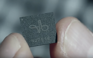
The Soli sensor is a fully integrated, low-power radar operating in the 60-GHz ISM band. In our journey toward this form factor, we rapidly iterated through several hardware prototypes, beginning with a large bench-top unit built from off-the-shelf components — including multiple cooling fans. Over the course of 10 months,
Read More
GLOBALFOUNDRIES today announced the signing of a memorandum of understanding to drive its next phase of growth in China. Through a joint venture with the government of Chongqing, the company plans to expand its global manufacturing footprint by establishing a 300mm fab in China. GLOBALFOUNDRIES is also investing in expanding
Read More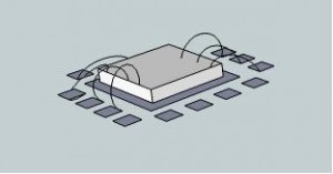
An integrated circuit package has the sole purpose of protecting and maintaining one or more integrated circuits. It is usually in the form of a plastic, glass, metal, or ceramic casing which creates a physical barrier of protection against things like impact and corrosion. Furthermore, it helps to hold contact
Read More
For the first time since 1993, the semiconductor industry is expected to witness a new number 1 supplier. Samsung first charged into the top spot in 2Q17 and displaced Intel, which had held the number 1 ranking since 1993. In 1Q16, Intel’s sales were 40% greater than Samsung’s, but in
Read More