

After years of legal struggles and law suits fights to defend their patents, Rambus decided to change its business model and enter into the market with its own brand.
Founded in 1990, Rambus was born to develop high-speed DRAM memory chips licensed to third companies that insert them into

Technology Trends
Process technology is progressing at a very fast pace and 16/14nm FinFET- based SOCs are available from various fabless companies. Significant investments in the development of advanced technology nodes are being made to ensure that future demands are met. This makes fab utilization of primary importance.

This article will give you a breakdown of the IP licensing model, describing the major players and the relationships between them. It is not designed to be a complete guide by any means and some parts might already sound familiar, but I hope it is a comprehensive overview that can
Read More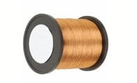
With the creeping rise in the price of gold, many microelectronics manufacturing companies have been looking for alternatives to reduce the cost of ball bonding. Recently, the trend has been to look into the use copper wire. However, there are many drawbacks to using copper wire, including the short shelf
Read More
UMC’s CEO, Po-Wen Yen, confirmed the drop of 5% on wafer shipment performance for the third quarter of 2015. The CEO justified this forecast by referring to a restricted market visibility and to weaknesses in the demand due to the uncertain economic environment. Not only, Po-Wen-Yen mentioned also the inventory
Read More
ARM has acquired Israel-based Sansa Security, a provider of hardware security IP and software for advanced system-on-chip components deployed in Internet of Things (IoT) and mobile devices. The company currently enables security in more than 150 million products a year and Sansa Security technology is deployed across a range of
Read More