


Today, ASIC design flow is a very solid and mature process. The overall ASIC design flow and the various steps within the ASIC design flow have proven to be both practical and robust in multi-millions ASIC designs until now.
Each and every step of the ASIC design flow has

This is a guest post by Dolphin Integration which provides IP core, EDA tool and ASIC/SoC design services
To reduce the Bill-of-Material (BoM) and to simplify their usage, System-on-Chips (SoC) become more and more complex due to the integration of a large number of features previously located on board. This increase

This is a guest post by PLDA which designs and sells intellectual property (IP) cores and prototyping tools for ASIC and FPGA
You are on a very strict schedule for your next chip. Not wanting to reinvent the wheel, you plan to go to an outside vendor for some of your
Read More
This is a guest post by Naman Gupta, a Static Timing Analysis (STA) engineer at a leading semiconductor company in India.
In accordance with the Moore’s Law, the number of transistors on integrated circuits doubles after every two years. While such high packing densities allow more functionality to be incorporated on
Read More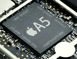
It’s no secret that Google, Amazon and Apple are heavily involved in the semiconductor industry. Apple itself is the biggest buyer of chips and estimated to buy 10% of chips sold worldwide. Google uses Intel’s CPUs in their server farms and represent alone 4% of Intel total sales.
Both

Chip production testing is probably the most underestimated task by ASIC development engineers. And yet, testing is an essential step with a direct impact on final chip cost.
Let’s start with the basics. Testing of chips is necessary because the chip manufacturing process cannot provide 100% yield. Silicon foundries