


Israeli start-up Glassify joined the IoT revolution and introduces the first beer glass integrating a semiconductor chip. The beer glass allows consumers to connect the glass to the smartphone using NFC technology.
According to the company the new beer glass allows consumer to enjoy a more personal
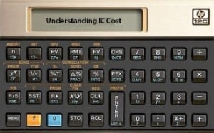
There have been many debates around the final cost of an IC. Over the years the misconception and failure to agree on what the calculated IC cost would be. The reason for this is that ICs are a simple concept anymore. Technology moves at an extremely fast pace and IC
Read More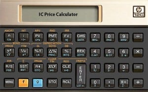
The IC Price Calculator is based on a standard price model that consists of all the required steps in IC manufacturing:
Wafer Price
Assembly/Package Price
Test Price
Yield
The IC Price Calculator is very easy to use and provides quick price estimate of IC price.
Read More
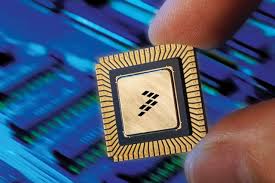
Optimal+, a leader in Manufacturing Intelligence solutions, today announced that it was selected by Freescale® Semiconductor to deliver their enterprise software suite to enhance the efficiency of their global manufacturing operations. In a move intended to improve the utilization of Freescale’s manufacturing equipment worldwide, the two companies signed a multi-year
Read More
Google is taking the next necessary steps towards the mobile phone market and plans to start developing and producing CPU chips for enabling a complete mobile phone eco system, to be combined with its successful Android operating systems.
Google has started in recent weeks talks with several processors
Read More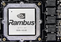
After years of legal struggles and law suits fights to defend their patents, Rambus decided to change its business model and enter into the market with its own brand.
Founded in 1990, Rambus was born to develop high-speed DRAM memory chips licensed to third companies that insert them into