

There are many ways to deliver, package and transport silicon products. Here’s a short primer that provides the basic facts regarding how silicon can be packed and delivered to ensure safe transportation with minimum damages.
There are two main options for receiving wafers from your foundry: tested or untested.
Untested wafers. This would be the “plain vanilla” delivery format. Wafers are delivered from the fab without being tested electronically. The wafers only go through visual inspection in order to detect visual defects, but are not functionally tested by any ATE.
Tested wafers. In this case, the wafers have been already tested and associated with a wafer map (file) indicating the pass and failed silicon dies. In this case, the tested wafers go through an electronic testing process (ATE), which is usually called Wafer Sort and conducted by a test house or the fab itself.
Some test houses still offer die inking instead of electronic wafer maps, but this method is not recommended today for wafer delivery. Inking is just more expensive than an electronic file.
Wafers Cassettes
Wafers (tested or untested) are delivered in wafer cassettes – plastic housing providing protection during transportation and storage. Cassettes can be stacked and are ideal for further post processing. Cassettes can be easily inserted into a various machines (for instance: wafer testing) for automatic handling. An ATE can access all the wafers in a cassette without any human intervention.
Wafers Carrier Boxes
For more robust packaging, wafers can be stored and shipped in carries (pizza) boxes. This method is not ideal for automated post processing because each box has to be manually opened and closed after processing. Wafer boxes have a smaller size than cassettes.
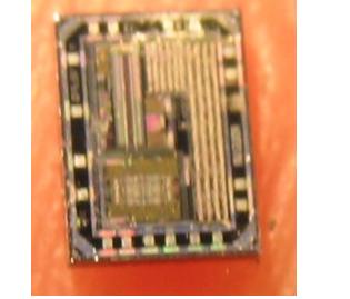
Die Delivery Formats
Silicon dies are separated from the wafer via a dicing or sawing process. Typically, wafers coming out of the foundry are approximately 750um thick to ensure maximum robustness during shipping. Before dicing wafers typically go through a back grinding (or backgrinding) process to thin down wafers to 75um to 50um. This step is mandatory in order to get the die into small packaging. The dicing process is performed by a mechanical sawing that saw in X and Y directions or by a laser cutter if more flexibility is required.
Known Good Die (KGD)
These are silicon dies which have been electronically tested before being placed in the carrier. A typical KGD is a result of a tested wafer that has been diced.
A KGD is the recommended method of delivery when the final product is a component consisting of multiple silicon dies. In this case, the known good dies are delivered to the assembly house from one or more foundries.
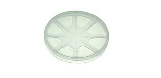
Dies on a waffle pack
Silicon dies can be delivered in a tray which is also known as waffle pack – a plastic tray with pockets that match the die size. A waffle pack has a lid and is delivered in an antistatic bag. Waffle packs are ideal for delivering small number of silicon dies, typically from a MPW process.
Dies on Blue Tape
Before wafer dicing, an adhesive tape is applied to the wafer together with a metal frame. After dicing the dies are glued to the membrane ready to be entered into the pick and place machine for assembly. The two most popular adhesive tapes are blue film and UV film. Blue film is approximately 1/3 of the cost of UV film

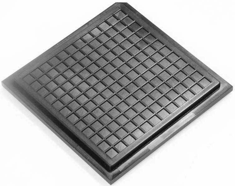
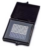
Dies on Gel Pack
Gel Pack provides more protection than a waffle pack and yet they can be easily removed. The carrier prevents die damage that can occur from contact with the edges or top surface of the carrier. Using surface tension, dies are held in place and protected, even if the carrier is tilted, or turned upside down.
Components Delivery Format
Components are packaged silicon dies.
Blind assembly is a term that describes untested silicon dies (in wafer format) that are about to be assembled into a package. In cases when the yield is high so that wafer testing is more expensive than the packaging cost of bad devices, the wafer testing step can be skipped.
These are components which are tested after the assembly process. After this step the components qualify to be assembled on the PCB.
Larger components such as BGA packages are shipped in a matrix tray that complies to the JEDEC standards. Typically, JEDEC trays have the same ‘x’ and ‘y’ outer dimensions and are easily stacked for storage and manufacturing. Components are also arranged in the trays to match industry standards.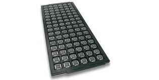
As indicated by its name, this is a method of covering parts in separate pockets in a long continuous plastic strip. The reel is a very common method for ‘feeding’ small components to automated PCB assembly equipment.
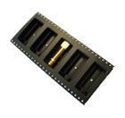
Sticks (or tubes) are constructed of rigid clear or translucent polyvinylchloride (PVC) material. The sticks have standard outlines that meet current industry standards, and protect components during shipping and handling. Sticks fit perfectly to feeder systems for automated assembly or testing.
This method involves a baking process for plastic packages such as BGA and QFN, to remove the moisture from these vulnerable devices and avoid a popcorn effect. The baking time is driven from the number of days or hours the components should be exposed (outside the pack) before being assembled on a PCB.
Need a price quote for your IC/SoC packaging? Get 3 quotes quickly using this form.
Get an indicative packaging cost range, then a detailed breakdown by email.


