


In a world hungry for efficient power, Silicon Carbide Semiconductors are the unsung heroes behind the scenes. From revolutionizing industrial machines to powering sophisticated electronics, their impact is both broad and deep. Prepare to discover the versatile applications that make silicon carbide semiconductors a cornerstone of modern technology.
This

We wrote before about multi project wafer benefits for IC designers of using MPW multi-project-wafer services.
Multi Project Wafer service is allowing companies to share the expensive mask cost. Essentially, Multi project wafer (MPW) services integrate onto silicon wafers several different integrated circuit designs from various teams. These designs
Mar. 12, 2024 —- The latest TrendForce report reveals a notable 7.9% jump in 4Q23 revenue for the world’s top ten semiconductor foundries, reaching $30.49 billion. This growth is primarily driven by sustained demand for smartphone components, such as mid and low-end smartphone APs and peripheral PMICs. The launch season for Apple’s latest
Read More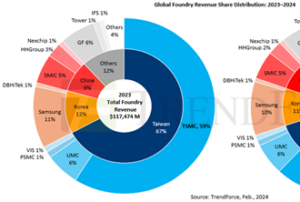
In their latest report TrendForce revealed that in 2023, Semiconductor foundry revenues hit US$117.47 billion, with TSMC capturing a dominant 60% share. This figure is expected to climb to around $131.65 billion in 2024, increasing TSMC’s share to 62%. Not only is TSMC leading in revenue, but it has also
Read More
February 20, 2024: Avnet ASIC Israel Ltd, (AAI) a leading provider of ASIC and SoC full turnkey solutions and a business division of Avnet Silica, an Avnet company (NASDAQ: AVT), has been appointed as a Value Chain Aggregator (VCA) by TSMC, the world’s leading silicon foundry. The appointment positions Avnet
Read More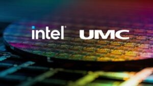
SANTA CLARA, Calif., and TAIPEI, Taiwan, ROC, Jan. 25, 2024 – Intel Corp. (Nasdaq: INTC) and United Microelectronics Corporation (NYSE: UMC; TWSE: 2303) (“UMC”), a leading global semiconductor foundry, today announced that they will collaborate on the development of a 12-nanometer semiconductor process platform to address high-growth markets such as mobile,
Read More