


GlobalFoundries is probably doing something right because China has set its eyes on GlobalFoundries with rumors of a possible imminent acquisition. Indeed, thanks to several strategical decisions, GlobalFoundries is offering today a unique portfolio, both CMOS and SiGe processes, cutting-end technology (14nm and 22FDSOI) and a global semiconductor manufacturing footprint.
Read More
China’s largest semiconductor foundry has successfully manufactured Qualcomm’s Snapdragon 410 processors using its 28nm technology.
The news came directly from the president of Qualcomm Incorporated, Derek Aberle, and Dr. Zixue Zhou, Chairman of SMIC, the company that just one year ago was announcing the collaboration with Qualcomm Technology.
Read More
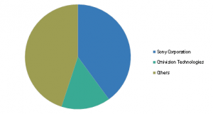
Image sensor, in today’s world, has become an important component for many devices that we use in our daily life. Smart phone and tablets are one of the most important devices that are used. The growing popularity of sharing photos over social media through mobile phones instead of carrying camera
Read More
UMC’s CEO, Po-Wen Yen, confirmed the drop of 5% on wafer shipment performance for the third quarter of 2015. The CEO justified this forecast by referring to a restricted market visibility and to weaknesses in the demand due to the uncertain economic environment. Not only, Po-Wen-Yen mentioned also the inventory
Read More
I recently read an interesting article “Intel’s cost cuts could give rivals higher ground: analysts” where the analysis claims that Intel Corp’s move to delay the launch of its next generation chip technology to 2017 may see the company lose ground to rivals Taiwan Semiconductor Manufacturing Co and Samsung Electronics
Read More
Taiwan Semiconductor Manufacturing Company (TSMC) has dropped its prices on 28nm and 20nm process technologies by 5-10% in hopes to secure additional orders from major companies which includes Qualcomm and MediaTek, according to DigiTimes. However, the reaction of 28nm prices will most likely affect AMD and Nvidia positively, who are
Read More