


Bob Colwell, Director of the Microsystems Technology Office (MTO) at the Defense Advanced Research Projects Agency (DARPA), recently made a compelling statement about the end of Moore’s Law: “When Moore’s Law ends, it will be economics that stops it, not physics. Follow the money.”
If we move beyond Moore’s

The ultimate ASIC calculator is available live on AnySilicon’s website. Together with our Die Per Wafer calculator this ASIC price calculator provides a very accurate final price for ASIC designs. Please note, we did not include shipping cost therefore you may want to add this to the total prices.
Read More
Die Per Wafer (DPW) online calculator is free and available live on AnySilicon website. The die per wafer calculator is simple to use and very accurate, however the results are estimates.
Now when you have the number of dies per wafer, you may want to consider:
See

Gordon Moore said‚ on the 40th anniversary of his law that “Moore’s law is really about economics.” What did he really mean by that? In 1965 when Gordon Moore put forth Moore’s law based on his observation, those years were Golden years of Free Market Capitalism in America. The entire decade
Read More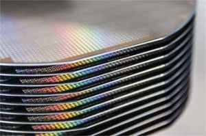
SEMICON West 2014 in San Francisco was a great place to meet bloggers in the semiconductor industry to get updated on the status of 450mm diameter silicon wafers. On one side, there is a good news about the unprecedented level of collaboration taking place between the design and construction professionals
Read More
Each year, top foundries are ranked by their sales, and you probably don’t need the table below to know who’s first.
But what if we look at the top foundries from the capacity angle? Each of the top foundries holds several production lines that address different technology nodes and wafer