Integrated circuits can fail for many different reasons. Some failures originate inside the semiconductor die, while others result from packaging, manufacturing, assembly, electrical overstress or the environment in which the device operates. Common IC failure mechanisms include electrostatic discharge (ESD), electrical overstress (EOS), electromigration, dielectric breakdown, interconnect defects, corrosion, contamination, thermal damage and mechanical or package-related failures. Identifying the visible damage, however, is not enough.
A semiconductor failure-analysis investigation should attempt to distinguish between:
For example, an IC may stop functioning because a metal interconnect has become electrically open. Physical analysis may reveal a void in the metal line, while further investigation indicates electromigration as the mechanism responsible for forming the void. Even then, the root cause may still need to be determined. Understanding this distinction is essential for effective semiconductor root-cause analysis.
For an overview of the complete subject, see:
Semiconductor Failure Analysis: The Complete Guide to IC Failure Analysis
For information about the investigation process, see:
Semiconductor Failure Analysis Process: From Failure to Root Cause
An IC failure mechanism is the physical, electrical, chemical or mechanical process that causes a semiconductor device to degrade or fail.
Examples include:
These terms are sometimes used interchangeably, but they describe different parts of the failure.
What the user or test system observes.
Examples:
How the device fails electrically or functionally.
Examples:
The physical abnormality found during analysis.
Examples:
The process responsible for producing the defect.
Examples:
Why the failure mechanism occurred in the first place.
The root cause might involve:
Consider the following example:
Symptom: IC stops operating
↓
Failure mode: Open circuit
↓
Physical defect: Void in metal interconnect
↓
Failure mechanism: Electromigration
↓
Root cause: Excessive current density in the interconnect
This distinction becomes particularly important when corrective action is required.
The table below summarizes several important semiconductor failure mechanisms and the techniques commonly used to investigate them.
| Failure Mechanism | Typical Symptoms / Damage | Common Analysis Techniques |
|---|---|---|
| Electrostatic Discharge (ESD) | Leakage, short circuit, junction or oxide damage | I-V analysis, EMMI, SEM, FIB |
| Electrical Overstress (EOS) | High current, burns, shorts, melted structures | EFA, EMMI, thermal imaging, SEM/FIB |
| Electromigration | Increased resistance, open circuit, sometimes short circuit | Electrical testing, SEM, FIB |
| Dielectric / Gate-Oxide Breakdown | Leakage, short circuit, parametric failure | I-V analysis, EMMI, nanoprobing, FIB/TEM |
| Metal Open or Short | Open circuit, leakage, functional failure | EFA, SEM, FIB |
| Via / Contact Failure | High resistance, open circuit, intermittent behavior | Nanoprobing, FIB, SEM |
| Corrosion | Leakage, increased resistance, open circuit, visible damage | Optical microscopy, SEM + EDS/EDX |
| Contamination | Leakage, shorts, corrosion, reliability degradation | SEM + EDS/EDX, surface analysis |
| Thermal Damage / Overheating | Parametric shift, leakage, burns, catastrophic failure | Thermal imaging, EFA, SEM |
| Package Delamination | Intermittent operation, package reliability failure | SAM, cross-section analysis |
| Bond-Wire Failure | Open or intermittent connection | X-ray, optical microscopy, SEM |
| Die-Attach Failure | Thermal problems, mechanical damage, reliability failure | SAM, X-ray, cross-section analysis |
| Solder-Joint Failure | Open circuit, intermittent connection, increased resistance | X-ray, cross-section analysis, SEM |
| Mechanical Cracking | Open circuit, leakage, intermittent or complete failure | Optical microscopy, SAM, SEM, cross-section analysis |
The exact FA technique depends on the device and the electrical signature. See IC Failure Analysis Techniques: A Complete Guide for a more detailed comparison.
Electrostatic Discharge, or ESD, occurs when accumulated electrostatic charge is suddenly transferred between objects at different electrical potentials. Semiconductor devices can be particularly sensitive to these very fast electrical events.
The EOS/ESD Association identifies several basic ways ESD can damage electronic devices, including a discharge directly to the device, a discharge from a charged device, and field-induced discharge events.
ESD can occur during:
Potential damage can involve:
A device damaged by ESD may exhibit:
The EOS/ESD Association also discusses the possibility of latent ESD-related degradation, although it explicitly notes that the concept of latent ESD failure remains technically controversial.
Typical techniques may include:
The objective is to correlate the electrical abnormality with physical damage consistent with an ESD event. However, analysts should be cautious about concluding that unusual physical damage automatically proves ESD.
Read more:
ESD Failure in Integrated Circuits: Causes, Analysis and Prevention
Electrical Overstress, or EOS, occurs when an electronic device experiences electrical conditions beyond the levels it can safely tolerate. EOS and ESD are related but not identical.
ESD generally involves a fast electrostatic discharge event. EOS is a broader category of damaging electrical stress and may involve excessive:
The EOS/ESD Association notes that EOS may result from application conditions such as a voltage on a supply pin exceeding the device’s absolute maximum rating.
Possible causes include:
Physical evidence may include:
Electrical symptoms can include:
The EOS/ESD Association emphasizes that distinguishing the actual origin of EOS damage can be difficult and may require cooperation between semiconductor suppliers and system customers.
A typical investigation may combine:
Electrical characterization
↓
EMMI or thermal localization
↓
SEM/FIB examination
↓
System and application review
The last stage is critical. Finding damage compatible with electrical overstress does not explain what caused the overstress.
Read more:
Electrical Overstress (EOS) Failure in ICs
Electromigration is an important long-term reliability mechanism in semiconductor interconnects. Current flow can contribute to movement of metal atoms within an interconnect. Over time, this can create material redistribution and void formation.
Potential consequences include:
Electromigration is strongly associated with interconnect reliability, particularly where high current density and temperature are present.
Electromigration-related failures may appear as:
Techniques may include:
A typical physical finding might be a void within an interconnect. But root-cause investigation should also consider:
Read more:
Electromigration in Integrated Circuits
Integrated circuits depend on extremely thin insulating layers to electrically separate structures. If a dielectric loses its insulating properties, unwanted current can flow through it.
Possible effects include:
Dielectric degradation can develop progressively under electrical stress. Reliability engineers may use accelerated stress testing to understand the lifetime of dielectric structures.
The specific breakdown physics varies depending on:
Possible analysis methods include:
For advanced semiconductor devices, the physical defect may be extremely small, making precise electrical localization important before TEM-level analysis.
Not every semiconductor reliability mechanism produces an immediate catastrophic failure. Some mechanisms gradually change transistor parameters over time. Bias Temperature Instability (BTI) is an important MOSFET aging mechanism.
Potential consequences include:
BTI is therefore different from a catastrophic metal short or bond-wire break. The device can remain functional while its electrical characteristics gradually move away from their original values. Electrical characterization is particularly important for analyzing this type of degradation.
Another transistor-aging mechanism involves energetic charge carriers creating or activating defects within semiconductor structures.
Potential effects can include changes in:
These failures may therefore initially appear as parametric degradation rather than catastrophic damage.
Advanced characterization can require:
Integrated circuits contain multiple layers of conductive interconnect. Failures within these structures can cause:
A conductor loses continuity. Possible physical causes include:
Two structures that should be electrically isolated become connected. Possible causes include:
Electrical Failure Analysis can first identify the open or short. FIB and SEM can then expose and inspect the relevant interconnect.
Read more:
Electrical Failure Analysis (EFA) of Integrated Circuits
and
Physical Failure Analysis (PFA) of Semiconductor Devices
Vias and contacts connect different conductive levels within an integrated circuit. As these features become smaller, even a tiny structural defect can significantly affect electrical resistance.
Failures can involve:
Typical electrical symptoms include:
A typical investigation may use:
Electrical fault localization
↓
FIB cross-section
↓
SEM
↓
TEM if required
This allows the analyst to inspect the exact via or contact identified electrically.
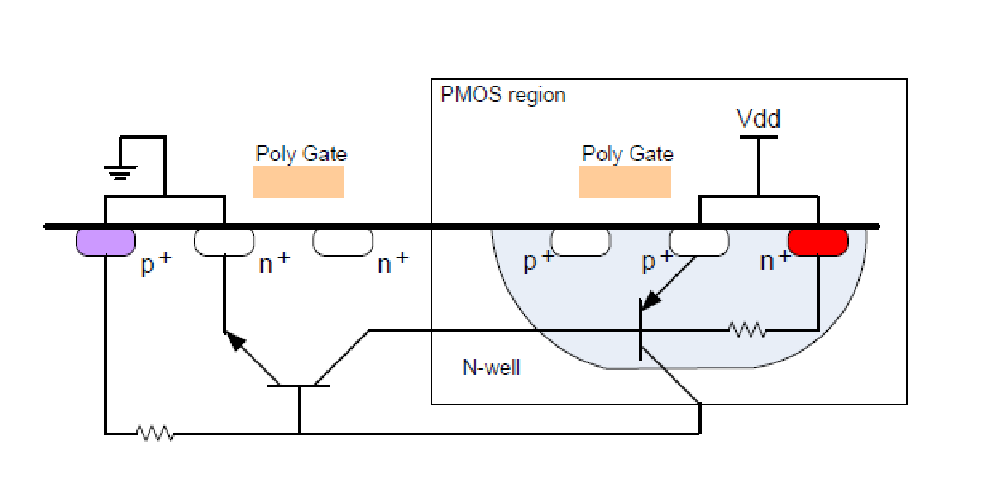
Latch-up is a condition in CMOS structures where parasitic device structures can create an unintended low-resistance current path. If the condition persists, excessive current can potentially damage the IC.
The EOS/ESD Association’s current technology roadmap discusses latch-up testing and notes its relationship to fast transient electrical-overstress conditions.
Possible symptoms include:
In some cases, latch-up itself may be recoverable when power is removed; in others, the resulting current can produce permanent EOS damage.
This is another example where the initiating event and resulting physical damage should be distinguished.
Semiconductor devices contain metals and interfaces that can be affected by chemical reactions.
Corrosion can be promoted by combinations of:
Possible effects include:
Possible methods include:
Contamination can originate during:
Examples can include:
Contamination does not always cause immediate failure. Depending on its location and composition, it can contribute to:
SEM can identify particle morphology, while EDS/EDX can provide local elemental information. For very shallow surface contamination or chemical-state analysis, techniques such as AES or XPS may be more suitable.
The important question is not simply:
“What material is present?”
but:
“Did this material cause the failure, and where did it come from?”
Temperature strongly affects semiconductor reliability. Excessive temperature can originate from:
Thermal stress can accelerate other mechanisms rather than acting independently. For example, elevated temperature can influence:
This means an FA investigation may need to distinguish between:
Thermal damage as the root problem
and
Heat produced by another electrical failure.
Thermal imaging can be particularly helpful for identifying abnormal heat generation before destructive analysis.
Wire bonds provide electrical connections between the semiconductor die and package in many conventional IC packages.
Potential bond-wire failures include:
Typical electrical symptoms include:
The investigation should determine whether the bond failure resulted from:
Read more:
The die-attach material provides mechanical and, in many devices, thermal connection between the semiconductor die and package or substrate.
Potential problems include:
Die-attach problems can be particularly significant in power semiconductor devices because thermal performance is critical.
Possible analysis techniques include:
Semiconductor packages contain multiple material interfaces. Differences in material properties and thermal expansion can create mechanical stress. Delamination occurs when layers or materials separate at an interface.
It may appear between:
Scanning Acoustic Microscopy is especially useful because it can detect interface abnormalities without first cutting through the package. Cross-sectioning can then provide direct physical examination of the interface.
Solder joints can fail because of:
Typical symptoms include:
Analysis techniques can include:
Mechanical failures can occur in:
Potential causes include:
Depending on the location, cracks may cause:
Methods such as SAM, optical microscopy, SEM and cross-section analysis can help identify the crack and its path.
It is useful to distinguish when failures occur during the product lifetime.
These occur relatively early and may be associated with:
Screening and qualification are often intended to identify populations with elevated early-failure risk.
These may result from:
These arise as device structures gradually degrade with accumulated stress.
Examples can include mechanisms such as:
It is important to note that “early life” and “wear-out” describe lifetime regions rather than single physical failure mechanisms.
No single microscope image normally proves the entire failure mechanism. A strong investigation combines evidence from several sources.
For example:
The failure mechanism should be consistent with all relevant evidence.
Consider an IC exhibiting excessive leakage current.
EFA confirms abnormal leakage between two nodes.
EMMI identifies a small electrically active region.
FIB exposes the region.
SEM reveals an abnormal conductive bridge.
EDS identifies unexpected material within the bridge.
The conductive material created an unintended current path.
Manufacturing records are investigated to determine where the contamination was introduced.
Notice how the investigation progresses from:
Leakage
to
bridge
to
contamination
to
source of contamination.
Stopping at the first physical observation would not provide a complete root-cause analysis.
Another IC develops increasing resistance before eventually failing open.
Electrical measurements confirm the open.
Fault localization identifies a metal interconnect.
FIB exposes the relevant region.
SEM reveals a void interrupting the conductor.
The defect morphology and operating history are consistent with electromigration.
Current density, temperature and design conditions are reviewed to determine why electromigration developed.
Again:
Void formation is the physical evidence.
Electromigration is the mechanism.
Excessive current density or another enabling condition may be the root cause.
Incorrectly identifying a failure mechanism can lead to the wrong corrective action. If damage caused by EOS is incorrectly classified as a semiconductor process defect, engineers may spend significant effort modifying a fabrication process that was not responsible. Likewise, if a package crack is treated only as a mechanical defect without investigating thermal cycling or material mismatch, the same failure may recur.
A good semiconductor failure-analysis investigation therefore asks:
Important semiconductor failure mechanisms include ESD, EOS, electromigration, dielectric breakdown, transistor-aging mechanisms, interconnect defects, corrosion, contamination, thermal damage and package-related mechanical failures.
The relevant mechanisms vary considerably between device technologies and applications.
ESD is a specific type of fast electrostatic discharge event.
EOS is a broader category of electrical overstress in which a device experiences electrical conditions beyond what it can safely tolerate.
The resulting physical damage can sometimes look similar, which is why root-cause identification can be challenging.
Electromigration involves current-driven redistribution of metal within semiconductor interconnect structures.
Void formation can eventually increase resistance or interrupt the electrical path.
Gate-dielectric reliability depends on the dielectric, electric field, temperature, device structure and defect population.
Yes. Contamination can contribute to leakage, corrosion, bridging and other reliability problems depending on the material and its location.
Yes.
Package-related failure mechanisms can include delamination, cracking, bond-wire failure, die-attach problems and solder-joint fatigue.
Electrical Failure Analysis is typically used to characterize and localize the problem, while Physical Failure Analysis identifies the physical defect.
The results are then correlated with manufacturing, design, reliability and application information to determine the failure mechanism and root cause.
Finding the failure mechanism is one of the most important steps in semiconductor failure analysis.
But it should not necessarily be the final step.
A complete investigation should progress from:
Failure symptom
↓
Failure mode
↓
Failure location
↓
Physical defect
↓
Failure mechanism
↓
Root cause
↓
Corrective action
For example:
Excessive supply current
↓
Internal short
↓
Damaged metal structure
↓
Electrical overstress
↓
Application-level voltage transient
↓
Improved system protection
This is the difference between simply documenting a failed semiconductor device and performing meaningful root-cause analysis.
If you have a failed semiconductor device and need to determine the failure mechanism or root cause, AnySilicon can help connect you with semiconductor failure-analysis companies and laboratories.
Typical capabilities may include:
Find a Semiconductor Failure Analysis Company
When requesting support, include the device type, package, observed electrical failure, available samples, operating conditions and any analysis already completed. This can help identify the most appropriate laboratory and analysis approach.