Simply defined, Latch-Up in VLSI is a functional chip failure associated with excessive current going through the chip, caused by weak circuit design. In some cases Latch-Up can be a temporary condition that can be resolved by power cycle, but unfortunately it can also cause a fatal chip failure.
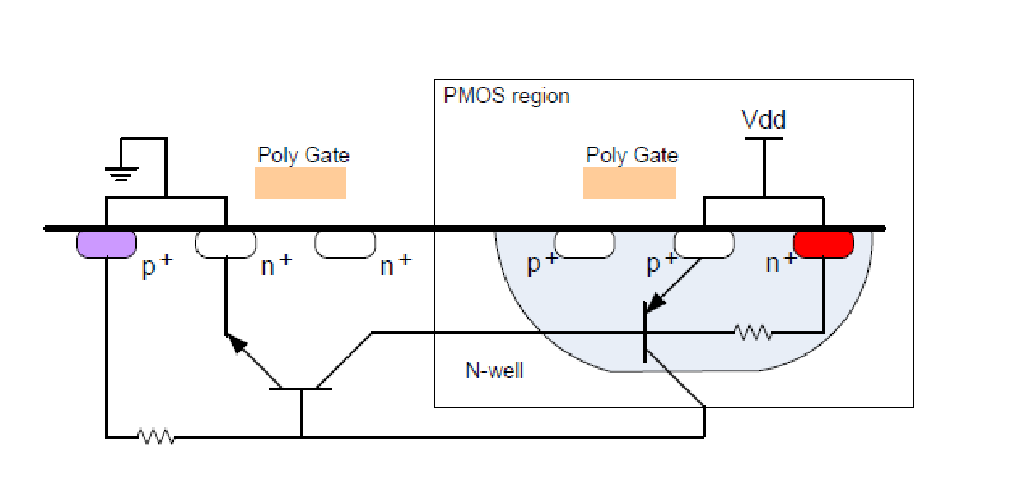
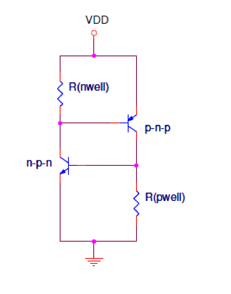
The following diagram is a drawing of a typical CMOS circuit. Notice the two transistors, NPN and PNP and their connection to VDD and GND supply rails. The two transistors are protected by resistors but if examined more closely, there’s an SCR device that could possibly be triggered.
In a latch-up conduction, the current flows from VDD to GND directly via the two transistors, causing the dangerous condition of a short circuit. The resistors are bypassed and thus excessive current flows from VDD to Ground.
There are many vendors that provide latch up testing services. The test is a series of attempts that trigger the SCR structure within the CMOS IC while the relevant pins are monitored for overcurrent behavior.
It’s recommended to take the very first samples from the engineering lot or MPW run and send them to a Latch-up testing lab. The lab will apply the maximum possible supply power and then inject current to the chip inputs and outputs while measuring if a Latch-up occurs by monitoring the supply current.
Do you need a price quote for Latch-up testing services? fill in this form and get price quotes within 1-2 days.