

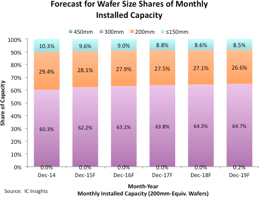
According to the latest report released by IC Insights, Global Wafer Capacity 2015-2019 shows a delay in 450mm wafers’ development and production in contrast to an increased 300mm wafers’ consumption by technology companies.
Judging from statistics, in fact, despite the huge economic incentives that would be generated on the production scale by adopting the 450mm wafers (up to 20% in savings), companies are facing incredible hard times to cope with the huge financial and technology obstacles that are afflicting the development and transition to the larger wafer.
Reports say it clear: the progress of the 450mm wafers is growing at an incredibly slow pace which hasn’t shown any attempt of improvement during 2014. Insiders’ forecasts are not too bright either. Indeed, the most influential operators of the industry say that the adoption of these wafers will happen only by 2020; maybe, in the best scenarios, some early adopters will start the production a couple of years before in order to test the market.
Another chart, always related to the mentioned report, shows the trend of IC fabs using the 300mm wafers. Before entering into the chart’s detail, it is worth to specify that this kind of products are used only inside high volume commodity type devices (like flash memories), image sensors, power management devices, complex logic and micro-component ICs with large die sizes and by foundries that can fill a 300mm fab by combining wafer orders from many sources. Getting back to the chart, it is shown that, after a short period decrease back in 2013, due to the closure of 3 large fabs, 300mm IC fabs were numbered 87 during 2014, expecting 23 more by the end of 2019. These number shows, once again, the evidence of a delayed entrance of 450mm wafers on the market.


