

Get the semiconductor daily news directly to you by subscribing to our email list. For ASIC designer and managers, staying updated with the latest news, technologies, and trends is crucial. Here are the lastest news from the semiconductor industry.

In today’s highly competitive market, businesses are continually seeking ways to gain an edge over their rivals. One possible strategy is using Application-Specific Integrated Circuits (ASICs). These specialized chips offer numerous benefits, allowing companies to create products that not only outperform the competition but also operate with better power efficiency
Read More
Imagine a world where every electronic device is tailored to its purpose with pinpoint precision. Custom ASICs, or Application-Specific Integrated Circuits, makes this a reality.
Custom ASICs represent a step beyond generic circuitry to meet unique demands. They offer customization levels from the architecture to the very silicon upon

Are you navigating the semiconductor qualification maze effectively? A lack of attention to ASIC qualification could lead to significant setbacks in cost and time for chip deployment. Our latest article sheds light on the critical importance of ASIC qualification and how it impacts your chip’s journey to high volume.
As

Santa Clara, CA – April 30, 2024 — Silvaco Group, Inc. (“Silvaco”), a provider of TCAD, EDA software, and SIP solutions that enable semiconductor design and AI through software and innovation, today announced it has launched the roadshow for its initial public offering (“IPO”) of 6,000,000 shares of its common stock.
Read More
This interview was held with Mayank Varshney, VP of Engineering, Mirafra Inc.
Please share with us a bird’s eye view about Mirafra Software Technologies?
Mirafra Software Technologies is possibly the largest Standalone Design Services company from India. Mirafra started couple of decades ago with a vision
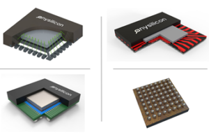
Introduction to Integrated Circuit Packaging
Integrated circuit packaging technologies have evolved throughout the years to the point where hundreds of IC package types are available today.
Most applications will require the more general, single-element packaging for integrated circuits and the other components such as resistors, capacitators, antenna etc.

This interview was held with Bram De Muer, CEO of ICsense
Tell me a bit about your background? How did you first get started with ICsense?
I am a microelectronics engineer by education. Engineering has always been in my blood, whether it was constructing novel

We wrote before about multi project wafer benefits for IC designers of using MPW multi-project-wafer services.
Multi Project Wafer service is allowing companies to share the expensive mask cost. Essentially, Multi project wafer (MPW) services integrate onto silicon wafers several different integrated circuit designs from various teams. These designs

Shanghai, China, March 28, 2024 — VeriSilicon (688521.SH) today announced its complete Bluetooth Low Energy (BLE) IP solution has achieved full compliance with LE Audio specification, including certifications for the LE Audio protocol stack and Low Complexity Communications Codec (LC3). This solution is applicable to mobile phones, Bluetooth earphones including True
Read More
Like architects shaping skylines, VLSI engineers are the masterminds behind the intricate circuits that power modern electronics. In the world of microelectronics, they play a pivotal role, crafting the very foundation upon which today’s technology thrives.
Core Responsibilities in Chip Creation: VLSI engineers are tasked with developing and refining