Silicon on Insulator (SOI) offers solutions to the increasing demand for faster, more efficient electronic devices that are critical in today’s digital age.
SOI technology separates the active layer of silicon from the bulk silicon substrate with an insulating layer, reducing parasitic capacitance and improving performance. As the industry grapples with the limitations of traditional bulk CMOS processes, the significance of SOI is becoming more apparent, particularly in applications demanding low power consumption and high speeds.
This article will explore the fundamentals of SOI, its advantages over bulk CMOS, and the various types of SOI devices. We will also delve into the fabrication methods, market outlook, and future potential of SOI technology, highlighting its role in shaping the next generation of electronics and beyond.
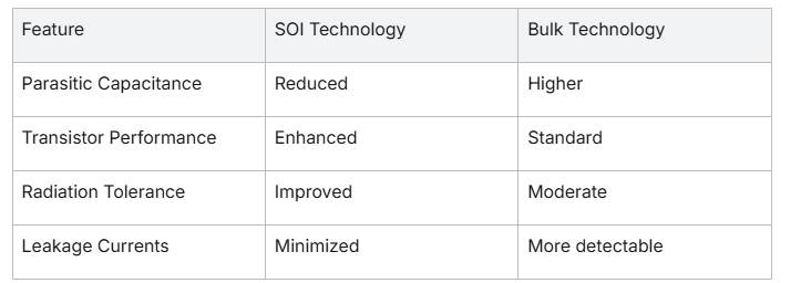
Silicon On Insulator (SOI) technology addresses many challenges in microelectronics. It improves transistor performance by reducing parasitic capacitance and leakage currents. The insulator layer, often silicon dioxide, separates the thin silicon layer from the silicon substrate. This separation minimizes these unwanted capacitances.
SOI is beneficial for short-channel effects, which are common in smaller transistors. It enhances radiation tolerance, making it useful in space and military applications. The mechanical properties of the insulator layer also support device structure stability.
By using oxide layers, SOI technology enhances the performance of microelectronic devices over bulk silicon wafers. This advancement is due to improvements in both device layers and junction capacitance. Device manufacturers benefit from a more reliable and efficient manufacturing process.
Moreover, SOI technology plays a crucial role in silicon photonics and bipolar device applications due to its unique properties.
SOI provides a balance for manufacturing methods that require enhanced performance and reliability in conventional silicon wafers.
Silicon On Insulator (SOI) technology is an innovation in the field of microelectronics. It involves a layer of silicon placed over an insulator layer, usually made of silicon dioxide. This setup minimizes parasitic capacitance, which can enhance transistor performance and reduce leakage currents. SOI technology is vital for producing high-speed and energy-efficient microelectronic devices.
Below are some key benefits of SOI technology:
SOI technology is widely used in manufacturing methods for silicon photonic devices, bipolar device applications, and more. It offers distinct advantages over conventional silicon wafers by using a silicon layer over an oxide layer. Device manufacturers rely on SOI for its ability to enhance device structure and performance.
Overall, the significance of SOI technology in modern electronics is profound, impacting device design and functionality.
Silicon On Insulator (SOI) and Bulk CMOS are two key technologies in chip manufacturing. Here’s a quick comparison:
SOI Technology
Bulk CMOS Technology
SOI’s advanced features such as reduced junction capacitance make it ideal for specialized device applications, while Bulk CMOS continues to appeal for its cost efficiency and broader application range.
Silicon On Insulator (SOI) technology offers several advantages over the traditional bulk CMOS process. Here are some key benefits:
These advantages make SOI a cutting-edge choice for device manufacturers aiming for high performance and reliability.
Silicon On Insulator (SOI) devices come in different types. Understanding these types helps in choosing the right technology for specific applications. Two primary types are fully depleted and partially depleted SOI devices.
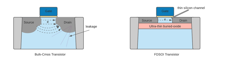
Fully depleted SOI (FDSOI) devices are known for their excellent electrical properties. The silicon layer in these devices is thin enough to be fully depleted of charge carriers. This results in reduced leakage currents and improved device performance. Such devices offer better control over the channel, which enhances the transistor’s speed and efficiency. These features make fully depleted SOI devices ideal for high-performance and low-power applications.
Benefits of Fully Depleted SOI Devices:
Partially depleted SOI devices have a thicker silicon layer. This layer is not fully depleted, which can lead to some leakage currents, but they are easier to manufacture. These devices are suitable for applications that do not require extreme low-power consumption. They provide a balance between performance and cost-effectiveness, making them popular in mainstream technology applications.
Key Features of Partially Depleted SOI Devices:
Understanding these types of SOI devices helps device manufacturers optimize their designs for various needs, ensuring efficient use of SOI technology.
Silicon On Insulator (SOI) technology offers significant advantages over traditional bulk silicon wafers. One key benefit is reduced parasitic capacitance, which improves device speed and lowers power consumption. This is especially important in microelectronic devices, where efficiency is crucial.
SOI technology uses an insulator layer, usually silicon dioxide, between the silicon substrate and the silicon film. This reduces leakage currents, enhancing transistor performance. It also minimizes short-channel effects in small devices, which often degrade performance in conventional silicon wafers.
Furthermore, SOI wafers improve radiation tolerance, making them ideal for space and military applications. The mechanical properties of SOI also allow for thinner device layers, which benefit modern compact device structures.
Advantages of SOI Technology:
In sum, SOI technology provides many advantages that cater to current demands for faster, more efficient microelectronic devices.
Silicon On Insulator (SOI) technology has numerous benefits, but its implementation presents several challenges.
Manufacturing Process: Creating SOI wafers involves complex manufacturing methods. The process requires forming a thin silicon layer on an insulator layer, typically silicon dioxide. Achieving uniform thickness across the silicon and insulator layers is difficult, affecting device performance.
Cost: SOI wafers are costlier than traditional bulk silicon wafers. This stems from the additional steps in the manufacturing process and the advanced equipment required.
Parasitic Capacitance: While SOI reduces parasitic capacitance, precise control of oxide layers is necessary. Inadequate control can lead to increased junction capacitance, impacting transistor performance.
Leakage Currents: SOI can reduce leakage currents, but improperly managed silicon film thickness may result in short-channel effects. This can limit improvements in device structure and performance.
Mechanical Properties: SOI wafers have different mechanical properties compared to bulk silicon. This can lead to issues during device fabrication, impacting reliability.
In summary, while SOI offers advantages like reduced leakage and better radiation tolerance, device manufacturers must navigate several obstacles. Optimum execution is vital for enhancing microelectronic device efficiency.
Silicon On Insulator (SOI) technology relies on advanced fabrication methods to create high-performance microelectronic devices. These methods ensure a precise arrangement of the silicon and insulator layers. The two primary techniques used are wafer bonding and layer transfer.
Wafer bonding is a key method in SOI fabrication. It involves attaching a silicon wafer to an insulator wafer, commonly silicon dioxide. This technique helps achieve the desired layer of silicon atop the insulating layer. The process requires extreme cleanliness and precise alignment. It can be challenging but essential for maintaining the mechanical properties and performance of the devices.
Wafer Bonding Process Steps:
Layer transfer is another crucial method. In this technique, a thin silicon layer is transferred onto an insulator substrate. It includes steps like ion implantation and layer splitting. The goal is to create a uniform silicon layer on the insulator.
Key Steps in Layer Transfer:
This approach helps manage the silicon layer’s thickness, which reduces issues like leakage currents and short-channel effects. Both wafer bonding and layer transfer methods are integral in producing reliable SOI wafers. They ensure device layers improve transistor performance and radiation tolerance while minimizing parasitic capacitance.
Silicon On Insulator (SOI) technology is vital for microelectronic devices. It uses a thin silicon layer laid over an insulator, often silicon dioxide (SiO2), to enhance device performance. This setup reduces parasitic capacitance and leakage currents, improving transistor performance.
Device manufacturers choose these materials for their favorable mechanical properties and reliable performance. SOI wafers are crafted through precise manufacturing methods, ensuring optimal transistor performance and reducing junction capacitance. Overall, SOI technology represents a significant improvement over conventional bulk technology.
Silicon On Insulator (SOI) technology plays a key role in modern circuit design. Designers must consider several factors to maximize performance and efficiency.
Key Considerations:
Benefits for Device Manufacturers:
By understanding these factors, designers can leverage SOI technology to create superior microelectronic devices.
Silicon On Insulator (SOI) technology offers enhanced device structures for microelectronic devices. It uses a thin layer of silicon on top of an insulator layer, often silicon dioxide. This setup reduces parasitic capacitance, boosting transistor performance and minimizing leakage currents. Here’s a look at SOI device structures:
SOI technology is preferred for its mechanical properties and efficiency in high-performance applications, such as silicon photonic devices and bipolar device applications. Its layers help in better junction capacitance control, making it appealing to device manufacturers. Using SOI wafers rather than conventional silicon wafers can result in significant performance improvements and cost savings.
Silicon on Insulator (SOI) wafers are essential in modern microelectronics. These wafers consist of a thin silicon layer atop an insulator layer, typically silicon dioxide. This structure reduces parasitic capacitance and improves device performance.
The manufacturing process of SOI wafers involves several steps:
These steps create a system with unique mechanical properties and improved radiation tolerance. It also reduces leakage currents and short-channel effects in devices.
Different techniques employed in SOI wafer production include:
SOI wafers are key in device manufacturing, enhancing transistor performance and enabling advanced applications like silicon photonic devices.
Silicon on Insulator (SOI) wafers are not just for standard microelectronic devices. They also find specialized applications in various fields. Their unique structure, which includes a silicon layer atop an insulator layer, brings many advantages
SOI wafers are ideal for Radio Frequency (RF) and mixed-signal electronics. These applications benefit from the reduced parasitic capacitance of SOI layers. This property leads to higher speed and better performance for RF devices. Reduced leakage currents also make SOI attractive for mixed-signal circuits. The increased radiation tolerance is a bonus for RF designs in harsh environments. Read more about RFSOI.
Benefits of SOI in RF Electronics:
Silicon photonics is another area where SOI shines. Telecommunications systems need fast, efficient, and small components. SOI structures help make this possible. The silicon film and insulator layer enhance light transmission and reduce energy loss. These features support the development of advanced photonic devices for faster data transmission.
Advantages of SOI in Photonics:
In summary, SOI technology offers significant benefits for specialized applications. It improves RF electronics and boosts silicon photonics for modern telecommunications.
Silicon On Insulator (SOI) technology is gaining momentum in the semiconductor market. This advanced method involves placing a thin silicon layer on top of an insulator layer, usually silicon dioxide. It improves transistor performance by reducing parasitic capacitance and leakage currents. SOI devices are more efficient than those made with bulk silicon wafers.
Market Drivers:
Manufacturing Trends:
The market is witnessing innovations in manufacturing methods. These are essential for creating thick-film SOI wafers with superior mechanical properties. Device manufacturers are leaning towards SOI for its better device structure flexibility.
SOI technology has a promising market outlook, with its improved device layers and insulator technology offering significant advantages over conventional silicon wafers.
Quantum computing is shaping the future of technology in remarkable ways. Here are some key trends influenced by this innovation:
These trends highlight the transformative potential of quantum computing across various sectors.
Characterizing Silicon On Insulator (SOI) is key in advancing microelectronics. SOI improves transistor performance due to its unique composition, involving a thin silicon layer on an insulator layer, typically silicon dioxide. Understanding its properties helps in optimizing device manufacturing and reducing parasitic capacitance.
These techniques help device manufacturers optimize the manufacturing process, reduce short-channel effects in transistor applications, and ensure radiation tolerance. Moreover, they guide the selection of appropriate manufacturing methods for both bulk technology and advanced SOI structures.
Silicon On Insulator (SOI) technology offers numerous performance benefits for microelectronic devices. By adding an insulator layer beneath the silicon film, SOI reduces leakage currents and improves device efficiency. This is crucial in reducing parasitic capacitance, which boosts transistor performance.
There are several advantages offered by SOI. These include:
SOI technology is redefining the standards for device manufacturers by providing a powerful alternative to conventional silicon wafer technology.
Silicon On Insulator (SOI) technology is a method of manufacturing integrated circuits (ICs) where transistors are built on an insulating substrate instead of a traditional silicon substrate. This insulating layer, typically silicon dioxide (SiO2), isolates transistors from each other, reducing parasitic effects and improving performance.
In bulk CMOS technology, both NMOS and PMOS transistors are fabricated on a single conductive silicon substrate. This can lead to parasitic effects like latch-up and reduced performance due to interactions between transistors. SOI technology, by placing transistors on an insulating layer, eliminates these issues, leading to better isolation and higher performance.
SOI technology offers several advantages over bulk CMOS:
There are two main types of SOI:
The insulating layer can be created using several methods:
Yes, SOI technology has a few challenges:
SOI technology is used in various applications where high performance and low power consumption are critical:
SOI technology is continually evolving and finding new applications as the demand for faster and more energy-efficient devices grows. Advancements in manufacturing techniques are reducing the cost of SOI wafers, making the technology more accessible for a wider range of applications. It is expected to play a crucial role in future semiconductor technology advancements.