
A wafer map is a critical tool used in the semiconductor manufacturing industry to visually display the good and bad dies found on wafers during the various process steps of chip production. These maps are integral to understanding and improving the fabrication process, ensuring the performance standards and quality of integrated circuits (ICs) are met.
Crafted typically after wafer test, a wafer map can be likened to a chart that highlights each chip on the entire wafer, marking the ones that are defective. These defects on wafer maps can range from minor deviations that slightly affect performance to major flaws that render a chip nonfunctional. This visual representation is critical for manufacturers to identify patterns of imperfections that may point towards systemic issues in the manufacturing process.
The use of wafer maps extends to predicting the performance of semiconductor devices before they are even deployed. Variations in performance indicated on these maps can be studied, and preemptive actions can be taken to rectify any found issues. By observing the consistency in performance across several wafers, engineers can adapt the manufacturing process to manufacture chips with higher yields.
In summary, a wafer map is a vital quality control instrument in the semiconductors process, representing visually the presence of defects and variations in performance of the wafers produced. They offer an essential glance into the invisible world of chip manufacturing, making the invisible, visible, and rectifiable. Through these maps, engineers can ensure that their products meet rigorous performance standards, maintain network performance, and sustain the ever-growing demands of technology
.
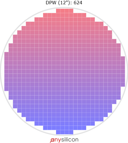
Die Per Wafer (DPW) is an important metric used in the semiconductor industry to determine the number of chips that can be produced on a single wafer. This metric is significant for manufacturers as it directly impacts the cost, throughput, and profitability of the production process.
The Die Per Wafer Calculator is a tool used to estimate the number of usable chips that can be obtained from a wafer. It takes into account various factors such as the size of the chips, the wafer size, and the presence of defects on the wafer. By inputting these variables into the calculator, manufacturers can gain valuable insights into the efficiency of their production process and optimize their operations accordingly. Try the AnySilicon Die Per Wafer Calculator.


